原著論文(レフェリー審査あり)
166報
論文リスト
2019年
1報
| 2019- 1. | Tsukasa Sugawara, Isao Hirano, Kensuke Kobayashi, Akira Kawai "Application of Polyimide Porous Membrane to Photopolymer Filter" J. Photopolymer Science and Technology, 32(6), 791-794 (2019) |
2018年
2報
| 2018- 1. | Tsukasa Sugawara, Jun Koshiyama, and Akira Kawai "Novel Fabrication of Three-Dimensional Homogeneous Microporous Polyimide Membrane" J. Photopolymer Science and Technology, 31(3), 437-440 (2018) |
| 2018- 2. | Tsukasa Sugawara, Hiroyoshi Sago, and Akira Kawai "In-Situ Observation of Permeation Behavior and Structural Analysis of Polyimide Membrane with Electrical Properties" J. Photopolymer Science and Technology, 31(6), 735-738 (2018) |
2017年
2報
| 2017- 1. | Natsumi Yagi and Akira Kawai "Three-Dimensional Analysis of Liquid Propagation at Microchannel Junction using ESEM" J. Photopolymer Science and Technology, 30(6), 709-714 (2017)[abstract] |
| 2017- 2. | Katsuaki Yamane and Akira Kawai "Application to Artificial Skin of Double Cone Tube Made of Acrylic Resin Formed by Micro Stereolithography" J. Photopolymer Science and Technology, 30(3), 345-350 (2017) [abstract] |
2016年
3報
| 2016- 1. | Hiroki Nakano, Kenta Takahashi, Akira Kawai "Negative pattern formation in positive resist layer by EB / UV hybrid lithography" J. Photopolymer Science and Technology, 29(4), 603-606 (2016) in perss. [abstract] |
| 2016- 2. | Hodaka Shirataki, Akira Kawai "In-situ Monitoring of TMAH Developer Intrusion into Resist Film by C-V Method" J. Photopolymer Science and Technology, 29(6), 817-822 (2016) [abstract] |
| 2016- 3. | Natsumi Yagi, Akira Kawai "Effect of Sub-Pattern on Guiding Liquid Propagation at Microchannel Junction" J. Photopolymer Science and Technology, 29(6), 833-834 (2016) [abstract] |
2014年
2報
| 2014- 1. | Yako Kunii, Akira Kawai "Tactile senses control by contacting a human finger with micro resist pattern arrangements" J. Photopolym. Sci. Technol., 27 (6) 691-694(2014) (IF: 1.055) [abstract] |
| 2014- 2. | Akira Kawai, Shogo Ohtani "Frequencydispersion of permittivity of SU-8 resist thin film" J. Photopolym. Sci. Technol., 27 (6) 711-712 (2014) (IF: 1.055) [abstract] |
2013年
7報
| 2013- 1. | Akira Kawai “Electrification on Condensation Surface of Micro Particles with Atomic Force Microscope (AFM)” J. Photopolymer Science and Technology, 26(6), 705-706 (2013). (IF: 0.908) [abstract] |
| 2013- 2. | Yuta Noguchi, Akira Kawai “Local Heating System Integrated with Platinum Micro Heater and Photopolymer Microfluidic Channel” J. Photopolymer Science and Technology, 26(6), 713-716 (2013). (IF: 0.908) [abstract] |
| 2013- 3. | Kazutoshi Otsuka, Kenta Takahashi, Akira Kawai “Fabrication of Micro Tube Array by Combining Positive with Negative Type Photoresists due to Solubility Difference in Developer” J. Photopolymer Science and Technology, 26(6), 717-720 (2013). (IF: 0.908) [abstract] |
| 2013- 4. | Yosuke Sakurai, Kenta Takahashi, Akira Kawai “Liquid Penetration Control of Photoresist/Perfluorosulfonic Acid (PFSA) Double Layer Structure by Hydrophobic Treatment” J. Photopolymer Science and Technology, 26(6), 727-732 (2013). (IF: 0.908) [abstract] |
| 2013- 5. | Yuta Noguchi, Kenta Takahashi, Akira Kawai “Micro Pinhole Formation in Photoresist Multilayer Structure controlled with Hydrophilic Treatment” J. Photopolymer Science and Technology, 26(6), 739-744 (2013). (IF: 0.908) [abstract] |
| 2013- 6. | Yosuke Sakurai, Daisuke Tanaka, Shunsuke Ohata, Akira Kawai “Fabrication and Durability of Single Chip Micro Direct Methanol Fuel Cell (SC-μDMFC) by Photolithography Process” J. Photopolymer Science and Technology, 26(6), 751-756 (2013). (IF: 0.908) [abstract] |
| 2013- 7. | Kenta Takahashi, Akira Kawai “Effect of Low Surface Tension Developer on Micro Bubble Removal from Resist Square Window Pattern” J. Photopolymer Science and Technology, 26(6), 765-768 (2013). (IF: 0.908) [abstract] |
2012年
4報
| 2012- 1. | Yuta Noguchi, Akira Kawai “Surface Stability of SU-8 film for Accurate Biopotential Detection” J. Photopolymer Science and Technology, 25(6), 719-722 (2012). (IF: 0.984) [abstract] |
| 2012- 2. | Yosuke Sakurai, Akira Kawai “Mechanical Stress Effect on Ionic Conductivity of Perfluorosulfonic Acid (PFSA) Film by Photolithography” J. Photopolymer Science and Technology, 25(6), 723-727 (2012). (IF: 0.984) [abstract] |
| 2012- 3. | Takashi Aiba, Akira Kawai “Micro Cantilever Motion in Micro Pattern Peeling by DPAT Method” J. Photopolymer Science and Technology, 25(6), 729-733 (2012). (IF: 0.984) [abstract] |
| 2012- 4. | Satoru Mori, Akira Kawai “Interfacial Microstructure of a Double-layer Cu Film Consisting of an Under-layer Deposited on SiO2 Substrate in Ar-10 vol% O2 and an Upper-layer Deposited in Pure Ar” J. Adhesion Soc. Japan, 48(1), 10-16 (2012). [abstract] |
2011年
2報
| 2011- 1. | Akira Kawai “Fluid Control MEMS constructed with Polymer Materials” J. Photopolymer Science and Technology, 24(5), 587-593 (2011). (IF: 0.904) [abstract] |
| 2011- 2. | Masayoshi Yamada, Akira Kawai “Micro Polymer Capsule Constructed with Micro Pillars Formed by Multi Laminating Method” J. Photopolymer Science and Technology, 24(6), 647-650 (2011). (IF: 0.904) [abstract] |
2010年
6報
| 2010- 1. | Satoru Mori, Akira Kawai “Low-Resistivity and Adhesive Sputter-Deposited Cu-Ca Films with an Intermediate Oxide Layer” Jpn. J. Appl. Phys., 49 (2010) p075804-1~8. (IF: 1.024) [abstract] |
| 2010- 2. | Tetsuya Ono, Akira Kawai “Free fall Mechanism of Micro Liquid Droplet” J. Photopolymer Science and Technology, 23(3), 363-366 (2010). (IF: 1.029) [abstract] |
| 2010- 3. | Masayoshi Yamada, Akira Kawai “Characterization of Resist Micro Pattern Adhesion by Applying Ultrasonic Vibration” J. Photopolymer Science and Technology, 23(3), 435-438 (2010). (IF: 1.029) [abstract] |
| 2010- 4. | Shunsuke Ohata, Akira Kawai “Dielectric Property of Solution Analyzed by using pn-junction Array” J. Photopolymer Science and Technology, 23(3), 367-370 (2010). (IF: 1.029) [abstract] |
| 2010- 5. | Junji Miyazaki, Nobuhito Toyama, Akira Kawai “Double Patterning Analysis Method by Emulation using a Double-Exposure Technique” Jpn. J. Appl. Phys., 49 (2010) p035201-1~6. (IF: 1.024) [abstract] |
| 2010- 6. | 山田昌佳、河合 晃、大澤義征、宝泉俊寛 「超音波プローブ振動法によるはんだバンプの付着性解析」 Microjoining and Assembly Technology in Electronics (Mate), 93-98 (2010) [abstract] |
2009年
5報
| 2009- 1. | Junji Miyazaki, Akira Kawai “Fidelity of Mask Shape and Use of a Correction Method in Anisotropic Si Wet Etching” J. Photopolymer Science and Technology, 22(6), 731-735 (2009). (IF: 0.780) [abstract] |
| 2009- 2. | Akihiro Takano, Akira Kawai “Analysis of self-standing structure composed by thick resist layer” J. Photopolymer Science and Technology, 22(5), 561-564 (2009). (IF: 0.780) [abstract] |
| 2009- 3. | Hiroki Sasazaki, Akira Kawai “Dielectric dispersion analysis of resist layer” J. Photopolymer Science and Technology, 22(3), 317-320 (2009). (IF: 0.780) [abstract] |
| 2009- 4. | Junji Miyazaki, Akira Kawai “Formation Mechanism of Micro Defect in Anisotropic Etching Analyzed by using Quasi-defect Pattern” J. Photopolymer Science and Technology, 22(3), 313-316 (2009). (IF: 0.780) [abstract] |
| 2009- 5. | Junji Miyazaki, Akira Kawai “Characterization of photomask substrate in optical lithography” J. Photopolymer Science and Technology, 22(5), 555-559 (2009). (IF: 0.780) [abstract] |
2008年
11報
| 2008- 1. | Daisuke Tanaka, Akira Kawai “Flowing control of micro bubbles in DFR micro fluidic channel formed on metal /insulator composite substrate” J. Photopolymer Science and Technology, 21(1), 63-68 (2008). (IF: 1.140) [abstract] |
| 2008- 2. | Akira Kawai, Daisuke Tanaka, Sachito Matsubara, Masayoshi Ogata, Kazutoshi Tachibana “Wetting control of polymer solution on roughened solid surfaces by wet-blast technique” J. Photopolymer Science and Technology, 21(1), 37-42 (2008). (IF: 1.140) [abstract] |
| 2008- 3. | Akira Kawai, Daisuke Tanaka, Tomotaka Ariga “Micro channel device composed by Dry film resist” J. Photopolymer Science and Technology, 21(1), 43-46 (2008). (IF: 1.140) [abstract] |
| 2008- 4. | Akira Kawai, Takashi Yamaji, Hiroshi Horiguchi “Adsorption of micro tip on various surface energy substrates” J. Photopolymer Science and Technology, 21(1), 85-88 (2008). (IF: 1.140) [abstract] |
| 2008- 5. | Takashi Yamaji, Akira Kawai “Non-contact deformation of resist micro pattern due to van der Waals Interaction” J. Photopolymer Science and Technology, 21(1), 89-94 (2008). (IF: 1.140) [abstract] |
| 2008- 6. | Akira Kawai, Masahito Hirano and Takashi Yamaji “Nano-scale Deformation of Resist Film Surface by Humidifying and Drying Processes” J. Photopolymer Sci. Technol., 21(6), 737-738 (2008). (IF: 1.140) [abstract] |
| 2008- 7. | Akira Kawai, Daisuke Tanaka “Micro Bubble Removal Depending on Glass Cleanness” J. Photopolymer Sci. Technol., 21(6), 727-728 (2008). (IF: 1.140) [abstract] |
| 2008- 8. | Akira Kawai, Takashi Yamaji “Internal Stress of Dry Film Resist in Multilayer Structure” J. Photopolymer Sci. Technol., 21(6), 725-726 (2008). (IF: 1.140) [abstract] |
| 2008- 9. | Akira Kawai, Junko Kawakami, Hiroki Sasazaki “Surface Energy change of Si(100) Wafer by Exposing to Air” J. Photopolymer Sci. Technol., 21(6), 739-740 (2008). (IF: 1.140) [abstract] |
| 2008-10. | Akira Kawai, Hotaka Endo and Daisuke Tanaka “Pinning Effect of Micro Bubbles adhered on Resist Substrate” J. Photopolymer Sci. Technol., 21(6), 753-754 (2008). (IF: 1.140) [abstract] |
| 2008-11. | Akira Kawai, Akihiro Takano “Spreading of Liquid Drop on Resist Film Surface” J. Photopolymer Sci. Technol., 21(6), 759-760 (2008). (IF: 1.140) [abstract] |
2007年
12報
| 2007- 1. | 河合 晃、川上喜章 「原子間力顕微鏡(AFM)による微細レジストパターン内の屈折率分布の解析」 日本接着学会誌、vol.43, No.4, 140-143 (2007). [abstract] |
| 2007- 2. | Akira Kawai, Kenta Suzuki “Bubbles Condensed at Water/resist Interface Analyzed by AFM” J. Photopolymer Science and Technology, 20(5), 673-678 (2007). (IF: 0.835) [abstract] |
| 2007- 3. | Akira Kawai, Norio Moriike “Visualization of stress distribution in resist film by surface plasma treatment” J. Photopolymer Science and Technology, 20(6), 783-784 (2007). (IF: 0.835) [abstract] |
| 2007- 4. | Masaki Yamanaka, Akira Kawai “Analysis of micro meniscus shape by light scattering” J. Photopolymer Science and Technology, 20(6), 781-782 (2007). (IF: 0.835) [abstract] |
| 2007- 5. | Akira Kawai, Takahiro Moriuchi “Non-contacting deformation (NCD) of line resist pattern due to interaction force with AFM tip” J. Photopolymer Science and Technology, 20(6), 777-780 (2007). (IF: 0.835) [abstract] |
| 2007- 6. | Kenta Suzuki, Akira Kawai “Micro bubbles formed on ArF excimer resist surface detected by tip scanning method” J. Photopolymer Science and Technology, 20(6), 805-806 (2007). (IF: 0.835) [abstract] |
| 2007- 7. | Akira Kawai, Junko Kawakami “Wetting analysis of hydrophobic substrate treated by HMDS primer” J. Photopolymer Science and Technology, 20(6), 815-816 (2007). (IF: 0.835) [abstract] |
| 2007- 8. | Akira Kawai, Masahito Hirano “Nano-wetting of DI-water analyzed by AFM” J. Photopolymer Science and Technology, 20(6), 813-814 (2007). (IF: 0.835) [abstract] |
| 2007- 9. | Shingo Kuroda, Tomohiro Goto, Osamu Tamada, Masakazu Sanada, Akira Kawai “Analysis of interface condition between BARC and resist film by FT-IR/ATR” J. Photopolymer Science and Technology, 20(6), 807-808 (2007). (IF: 0.835) [abstract] |
| 2007-10. | Kazutoshi Kurano, Takahiro Kishioka, Yoshiomi Hiroi, Takuya Ohashi, Akira Kawai “Peeling analysis of ArF resist pattern on BARC by using AFM” J. Photopolymer Science and Technology, 20(6), 825-826 (2007). (IF: 0.835) [abstract] |
| 2007-11. | Kazutoshi Kurano, Takahiro Kishioka, Yoshiomi Hiroi, Takuya Ohashi, Akira Kawai “Deformation analysis of ArF resist pattern by using AFM” J. Photopolymer Science and Technology, 20(6), 827-828 (2007). (IF: 0.835) [abstract] |
| 2007-12. | Harumitsu Kubota, Akira Kawai “Native oxide growth on Si(100) surface in liquid environment” J. Photopolymer Science and Technology, 20(6), 823-824 (2007). (IF: 0.835) [abstract] |
2006年
8報
| 2006- 1. | Akira Kawai, Takahiro Moriuchi, Takayoshi Niiyama, Takahiro Kishioka, Daisuke Maruyama,
Yasushi Sakaida, Takashi Matsumoto “Adhesion improvement of ArF resist pattern depending on BARC material” Microelectronic Engineering, 83, 659-662 (2006). (IF: 1.398) [abstract] |
| 2006- 2. | Akira Kawai, Hotaka Endo, Tomotaka Ariga “Condensation mechanism of microbubbles depending on DFR pattern design” Microelectronic Engineering, 83, 1167-1169 (2006). (IF: 1.398) [abstract] |
| 2006- 3. | Akira Kawai, Kenta Suzuki “Removal mechanism of nano-bubble with AFM for immersion lithography” Microelectronic Engineering, 83, 655-658 (2006). (IF: 1.398) [abstract] |
| 2006- 4. | Takayoshi Niiyama, Akira Kawai “Micro wetting system by controlling pinning and capillary forces” Microelectronic Engineering, 83, 1280-1283 (2006). (IF: 1.398) [abstract] |
| 2006- 5. | 安江孝夫、河合 晃 「走査型プローブ顕微鏡によるシリコン酸化膜の経時絶縁破壊特性」 日本表面科学会誌、27 (4) 49-54 (2006). [abstract] |
| 2006- 6. | Mitsuru Sato and Akira Kawai “Topcoat characterization for immersion lithography by fluoric acid etching on silicon substrate” J. Photopolymer Sci. Technol., 19(5), 601-611 (2006). (IF: 1.222) [abstract] |
| 2006- 7. | Takayoshi Niiyama and Akira Kawai “Formation factors of watermark for immersion lithography” Jpn. J. Appl. Phys. 45, 5383-5387 (2006). (IF: 1.222) [abstract] |
| 2006- 8. | Akira Kawai and Kenta Suzuki “Effect of low surface tension liquid on pattern collapse analyzed by observing dynamical meniscus observation” Jpn. J. Appl. Phys., 45, 5429-5434 (2006). (IF: 1.222) [abstract] |
2005年
5報
| 2005- 1. | Atsushi Ishikawa, Akira Kawai “Condensation of Nano-Size Polymer Aggregates by Spin Drying” J. Adhesion and Interface, vol.6 (1) 7-10 (2005). (IF: 1.024) [abstract] |
| 2005- 2. | Akira Kawai “Condensation behavior of nanoscale bubbles on ArF excimer resist surface analyzed by atomic force microscope” J. Photopolymer Sci. Technol., 18(3), 349-354 (2005). (IF: 0.859) [abstract] |
| 2005- 3. | Takayoshi Niiyama, Akira Kawai “Interaction analysis of DI-water / Air / ArF resist system using atomic force microscope” J. Photopolymer Sci. Technol., 18(3), 373-380 (2005). (IF: 0.859) [abstract] |
| 2005- 4. | Akira Kawai, Takahiro Moriuchi “Deflection analysis of micro cantilever due to water vapor adsorption” J. Photopolymer Sci. Technol., 18 (3), 681-682 (2005). (IF: 0.859) [abstract] |
| 2005- 5. | Akira Kawai, Kenta Suzuki “Dot pattern collapse due to Laplace force analyzed by dynamical meniscus model” J. Photopolymer Sci. Technol., 18(3), 679-680 (2005). (IF: 0.859) [abstract] |
2004年
12報
| 2004- 1. | Akira Kawai “Influence of moving speed of AFM tip on peeling strength of micro resist pattern” J. Adhes. Soc. Technol. 40, 11-13 (2004). [abstract] |
| 2004- 2. | 河合 晃、大澤義征 「角度制御型シェアモード剥離法」 Microjoining and Assembly Technology in Electronics, p77-82 (2004). [abstract] |
| 2004- 3. | Akira Kawai “Cohesion property of resist pattern surface analyzed by tip indentation method” J. Photopolymer Sci. Technol., 17(3), 441-448 (2004). (IF: 1.024) [abstract] |
| 2004- 4. | Takayoshi Niiyama and Akira Kawai “Interaction force analysis of resist film surface in water vapor” J. Photopolymer Sci. Technol., 17(3), 453-456 (2004). (IF: 1.024) [abstract] |
| 2004- 5. | Atsushi Ishikawa, Makoto Sakata and Akira Kawai “Meniscus analysis in micro gap during liquid drying process” J. Photopolymer Sci. Technol., 17(3), 457-460 (2004). (IF: 1.024) [abstract] |
| 2004- 6. | Akira Kawai, Masahito Hirano and Takayoshi Niiyama “Analysis for drying behavior of rinse water depended on resist pattern arrangement” J. Photopolymer Sci. Technol., 17(3), 461-464 (2004). (IF: 1.024) [abstract] |
| 2004- 7. | Atsushi Ishikawa, Takashi Tanji and Akira Kawai “Cohesion property of polymer aggregate depending on hardening treatment” J. Photopolymer Sci. Technol., 17(1), 99-102 (2004). (IF: 1.024) [abstract] |
| 2004- 8. | Akira Kawai, Akihiko Seki and Hotaka Endo “Viscous finger pattern formed in photoresist film during heat treatment” J. Photopolymer Sci. Technol., 17(1), 103-104 (2004). (IF: 1.024) [abstract] |
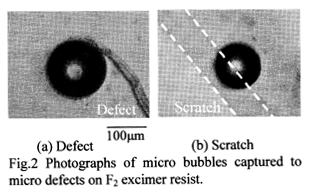
| 2004- 9. | Hotaka Endo and Akira Kawai “Micro bubbles captured at micro defect on resist film” J. Photopolymer Sci. Technol., 17(1), 105-106 (2004). (IF: 1.024) [abstract] |
| 2004-10. | Masaki Yamanaka, Akira Okada and Akira Kawai “Pinning effect of microliquid drop on geometrical complex substrates composed with different surface energy materials” J. Vac. Sci. & Technol. B22(6), Nov/Dec 3525-3527 (2004). (IF: 1.341) [abstract] |
| 2004-11. | Atsushi Ishikawa, Takashi Tanji, Akira Kawai “Determination of Young's modulus of polymer aggregate based on Hertz theory” J. Photopolymer Sci. Technol., 17(5), 715-718 (2004). (IF: 1.024) [abstract] |
| 2004-12. | Hotaka Endo, Akira Kawai “Adhesion mechanism of micro bubbles on ArF and F2 excimer resists” J. Photopolymer Sci. Technol., 17(5), 713-714 (2004). (IF: 1.024) [abstract] |
2003年
10報
| 2003- 1. | Akira Kawai, Daisuke Inoue “Effect of Thermal Stress on Peel Property of Line Resist Pattern Analyzed by Atomic Force Microscope (AFM)” J. Adhes. Soc. Technol. 39, 107-109 (2003). [abstract] |
| 2003- 2. | Daisuke Inoue, Akira Kawai “Peeling Analysis of Resist line Pattern of 170nm Width Due To Crack Formation by using Atomic Force Microscope Tip” Surface and Coating Technology, 169-170, pp.311-315 (2003). (IF: 1.410) [abstract] |
| 2003- 3. | Akira Kawai, Daisuke Inoue “Van der Waals interaction between Si surface and micro tip apex treated with hexamethyldisilazane (HMDS)” J. Adhes. Soc. Technol. 39, 255-258 (2003). [abstract] |
| 2003- 4. | Akira Kawai “Cohesion property of resist micro pattern analyzed by using atomic force microscope (AFM)” J. Photopolymer Sci. Technol., 16(3), 381-386 (2003). (IF: 1.062) [abstract] |
| 2003- 5. | Naotaka Kubota, Tomohiko Hayashi, Takeshi Iwai, Hiroshi Komano, Akira Kawai “Advanced resist design using AFM analysis for ArF lithography” J. Photopolymer Sci. Technol., 16(3), 467-474 (2003). (IF: 1.062) [abstract] |
| 2003- 6. | Akira Kawai “Adhesion of ArF Excimer Resist Pattern Depending on Heating Temperature Analyzed by Atomic Force Microscope” J. Adhes. Soc. Technol. 39, 423-425 (2003). [abstract] |
| 2003- 7. | Akira Kawai, Yuji Sawanaga “Condensation control of micro particles by charge deposition method” J. Photopolymer Sci. Technol., 16(5), 669-670 (2003). (IF: 1.062) [abstract] |
| 2003- 8. | Akira Kawai, Junko Kawakami “Characterization of SiO2 surface treated by HMDS vapor and O2 plasma with AFM tip” J. Photopolymer Sci. Technol., 16(5), 665-668 (2003). (IF: 1.062) [abstract] |
| 2003- 9. | Masahito Hirano, Akira Kawai “Adhesion of AFM tip to resist surface due to Laplace force” J. Photopolymer Sci. Technol., 16(5), 663-664 (2003). (IF: 1.062) [abstract] |
| 2003-10. | Takayoshi Niiyama, Yuji Sawanaga, Akira Kawai “Determination of electrified area formed by AFM lithography” J. Photopolymer Sci. Technol., 16(5), 661-662 (2003). (IF: 1.062) [abstract] |
2002年
9報
| 2002- 1. | Akira Kawai, Takato Abe “Analysis of Pattern Collapse of Electron Beam Resist Ranging from 60 to 152 nm Width with Atomic Force Microscope Tip” J. Adhesion Soc. Japan, 38 16-19 (2002). [abstract] |
| 2002- 2. | 河合 晃 「探針の吸着力測定による水蒸気の凝縮性解析」 日本接着学会誌、38, 50-53 (2002). [abstract] |
| 2002- 3. | 河合 晃 「水蒸気吸着に伴う微細カンチレバーの撓み変位の解析」 日本接着学会誌、38, 169-172 (2002). [abstract] |
| 2002- 4. | Akira Kawai “Adhesion and Cohesion Properties of Dot Resist Patterns Ranging from 84 to 364 nm Diameter Analyzed by Direct Peeling Method with Atomic Force Microscope Tip” J. Photopolymer Science & Technology, 15(1), 121-126 (2002). (IF: 1.062) [abstract] |
| 2002- 5. | Akira Kawai, Daisuke Inoue “Van der Waals Interaction between Polymer Aggregates and Substrate Surface Analyzed by Atomic Force Microscope (AFM)” J. Photopolymer Science & Technology, 15(1), 127-132 (2002). (IF: 1.062) [abstract] |
| 2002- 6. | Akira Kawai “Cohesion Property of Polymer Aggregates in Resist Pattern Analyzed by Atomic Force Microscope (AFM)” J. Photopolymer Science & Technology, 15(3), 371-376 (2002). (IF: 1.062) [abstract] |
| 2002- 7. | Akira Kawai, Daisuke Inoue “Peeling Property of Resist Pattern in Water Analyzed by Atomic Force Microscope” J. Photopolymer Science & Technology, 15(5), 757-758 (2002). (IF: 1.062) [abstract] |
| 2002- 8. | Akira Kawai “Resist Pattern Peel due to Resonance Effect of Micro Tip” J. Photopolymer Science & Technology, 15(5), 759-760 (2002). (IF: 1.062) [abstract] |
| 2002- 9. | Hideaki Yoshida, Tadashi Nakamura, Yoshiaki Kawakami, Akira Kawai “Establishment of Eaves Forming Model by Analysis of the Interface Energies at the Threefold of Cu/DFR/Ni Plating Solution” J. Adhesion Soc. Japan, 38, 413-419 (2002). [abstract] |
2001年
12報
| 2001- 1. | 河合 晃、堀口博司 「原子間力顕微鏡を用いた微細探針と無機固体表面間のHamaker定数解析」 日本接着学会誌、37, 146-149 (2001). [abstract] |
| 2001- 2. | Akira Kawai, Norio Moriike “Analysis of Pattern Collapse of ArF Excimer Laser Resist by Direct Peeling Method with Atomic Force Microscope Tip” Microelectronic Engineering, vol.57-58, pp683-692 (2001). (IF: 0.705) [abstract] |
| 2001- 3. | Akira Kawai, Norio Moriike “Adhesion and Cohesion Analysis of ArF/SOR Resist Patterns with Microtip of Atomic Force Microscope (AFM)” J. Photopolymer Science and Technology, 14(4), 507-512 (2001). (IF: 1.062) [abstract] |
| 2001- 4. | Akira Kawai, Takato Abe “Direct Measurement of Resist Pattern Adhesion on the Surface with Silane-coupling Treatment by Atomic Force Microscope (AFM)” J. Photopolymer Science and Technology, 14(4), 513-518 (2001). (IF: 1.062) [abstract] |
| 2001- 5. | 原 朋敬、小泉延恵、河合 晃 「Glass/レジスト/Cu/Al/Glass多層構造の破壊特性解析」 日本接着学会誌、37, 303-308 (2001). [abstract] |
| 2001- 6. | 阿部貴人、河合 晃 “原子間力顕微鏡(AFM)を用いた線幅60nmのラインレジストパターンの弾性解析” 日本接着学会誌、37, 353-357 (2001). [abstract] |
| 2001- 7. | Akira Kawai, Norio Moriike “Resist Hardening by Electron Beam Irradiation Analyzed by Atomic Force Microscope” J. Photopolymer Science and Technology, 14(5), 751-752 (2001). (IF: 1.062) [abstract] |
| 2001- 8. | Akira Kawai “Collapse of Dot Patterns Formed on Various Substrates analyzed by Tip Scanning Method” J. Photopolymer Science and Technology, 14(5), 723-724 (2001). (IF: 1.062) [abstract] |
| 2001- 9. | Akira Kawai, Yoshihisa Kaneko “Estimation of Young’s Modulus of Resist Pattern by using Atomic Force Microscope” J. Photopolymer Science and Technology, 14(5), 731-734 (2001). (IF: 1.062) [abstract] |
| 2001-10. | Akira Kawai, Yoshiaki Kawakami “DUV Hardened Layer of Resist Dot Pattern Detected by Tip Indentation Method” J. Photopolymer Science and Technology, 14(5), 749-750 (2001). (IF: 1.062) [abstract] |
| 2001-11. | Akira Kawai, Yoshihisa Kaneko “Fatigue Property of Resist Micro Pattern Analyzed by Atomic Force Microscope Tip” J. Photopolymer Science and Technology, 14(5), 701-702 (2001). (IF: 1.062) [abstract] |
| 2001-12. | 磯部 亮、河合 晃 「微細周期パターン上へのプラズマ重合膜の堆積特性」 日本接着学会誌、37, 433-436 (2001). [abstract] |
2000年
8報
| 2000- 1. | Akira Kawai “Collapse Behavior of Organic Dot-Pattern Analyzed by the Tip Indentation Method” J. Adhesion Soc. Japan, 36, 23-27 (2000). [abstract] |
| 2000- 2. | 河合 晃、川上喜章 “原子間力顕微鏡(AFM)を用いた微細探針走査法によるフォトレジスト微細パターンの接着性解析” 日本接着学会誌、36, 2-9 (2000). [abstract] |
| 2000- 3. | Akira Kawai, Yoshihisa Kaneko “Analysis of Resist Pattern Collapse by Direct Peeling Method with Atomic Force Microscope Tip” Jpn. J. Appl. Phys., 39, 1426-1429 (2000). (IF: 1.157) [abstract] |
| 2000- 4. | 河合 晃 “固体表面での微細探針の吸着力解析” 日本接着学会誌、36, 131-135 (2000). [abstract] |
| 2000- 5. | 河合 晃 “マイカへき開表面での微細探針の摩耗に伴う吸着力変化” 日本接着学会誌、36, 172-175 (2000). [abstract] |
| 2000- 6. | 森池教夫、河合 晃 “原子間力顕微鏡を用いた一括破壊試験法による有機ドットパターンの付着挙動解析” 日本接着学会誌、36, 295-301 (2000). [abstract] |
| 2000- 7. | 森池教夫、河合 晃 “原子間力顕微鏡を用いた微細レジストドットパターンの疲労解析” 日本接着学会誌、36, 404-407 (2000). [abstract] |
| 2000- 8. | Akira Kawai “Collapse Behavior of KrF Resist Line Pattern Analyzed with Atomic Force Microscope Tip” Jpn. J. Appl. Phys., 39, 7044-7048 (2000). (IF: 1.058) [abstract] |
1999年
2報
| 1999- 1. | Akira Kawai “Collapse Behavior of Micro Resist Pattern Analyzed by Tip Indentation Method with Atomic Force Microscope” J. Vac. Sci. & Technol. B17, 1090-1093 (1999). (IF: 1.687) [abstract] |
| 1999- 2. | 河合 晃 「Cu/Al多層膜構造の破壊強度に及ぼすAl自然酸化膜の影響」 日本接着学会誌、35, 558-561 (1999). [abstract] |
1998年
5報
| 1998- 1. | 河合 晃 「10nm以下のAu薄膜の成長挙動と接触角変化」 日本接着学会誌、34, 209-213 (1998). [abstract] |
| 1998- 2. | 河合 晃 「ミクロンサイズの格子型基板を用いた液滴平面形状の制御」 日本接着学会誌、34, 226-228 (1998). [abstract] |
| 1998- 3. | Akira Kawai “Characterization of Fall Angle of Water Drop based on Surface Energy Components” J. Adhesion. Soc. Japan, 34, 191-193 (1998). [abstract] |
| 1998- 4. | 河合 晃、岡田 彰 「異種材料で構成された格子状基板上での液滴の接触角」 日本接着学会誌、34, 22-25 (1998). [abstract] |
| 1998- 5. | 堀口博司、河合 晃 「AFM探針とポリスチレンラテックス(直径42nm~1μm)凝集粒子間の付着力解析 -DMT理論に基づく微粒子系の相互作用力の補正式-」 日本表面科学会誌、19, 491-497 (1998). [abstract] |
1997年
4報
| 1997- 1. | 河合 晃 「原子間力顕微鏡(AFM)によるフォトレジスト膜表面の摩擦挙動解析(周期パターンの歪検出方式)」 日本接着学会誌、33, 465-471 (1997). [abstract] |
| 1997- 2. | 河合 晃、芦田安立 「AFM微細探針によるAu表面の弾性および吸着特性」 日本接着学会誌、33, 395-397 (1997). [abstract] |
| 1997- 3. | Wataru Wakamiya, Makoto Hirayam, Akihiko Yasuoka, Akira Kawai “Refractive Index Distribution in Photoresist Thin Film Formed by the Spin Coating Method” Jpn. J. Appl. Phys., 36, L1622-L1624 (1997). (IF: 1.261)[abstract] |
| 1997- 4. | 河合 晃、小泉延恵 「溶剤蒸発に伴うレジスト膜の粘性指状変形と接着性」 日本接着学会誌、33, 434-437 (1997). [abstract] |
1996年
6報
| 1996- 1. | 河合 晃、熊谷武司、高田雅介 「遷移金属薄膜上に形成したBaTiO3薄膜の熱処理時の接着挙動」 日本接着学会誌、32, 404-409 (1996). [abstract] |
| 1996- 2. | Akira Kawai “Measuring the Thermal Properties of Photoresist Thin Films Using Atomic Force Microscopy” Thin Solid Films, 273, 308-311 (1996). (IF: 1.890) [abstract] |
| 1996- 3. | 河合 晃 「スパッタリングで形成したAuおよびPtの大気中放置に基づく表面自由エネルギー変化」 日本接着学会誌、32, 39-43 (1996). [abstract] |
| 1996- 4. | Akira Kawai, Takeshi Kumagai and Masasuke Takata “Correlation between Surface Free Energy and Dielectric Constant of BaTiO3 Thin Film” J. Adhesion Society of Japan, 32, 221-223 (1996). [abstract] |
| 1996- 5. | Wataru Wakamiya, Makoto Hirayama, Akihiko Yasuoka and Akira Kawai “Adhesion Improvement of Photoresist on TiN/Al Multilayer by Ozone Treatment” Jpn. J. Appl. Phys., 35, L1227~L1229 (1996). [abstract] |
| 1996- 6. | 若宮 亙、平山 誠、安岡晶彦、河合 晃 「フォトレジスト膜へのアルカリ水溶液の浸透と接着性」 日本接着学会誌、32, 294-297 (1996). [abstract] |
1995年
11報
| 1995- 1. | 永田一志、河合 晃 「Al薄膜の表面粗さとレジスト微細パターンの接着性」 日本接着学会誌、31, 44-48 (1995). [abstract] |
| 1995- 2. | 永田一志、河合 晃 「フォトレジスト膜の残留歪みと接着性に及ぼす溶剤の効果」 日本接着学会誌、31, 187-191 (1995). [abstract] |
| 1995- 3. | 河合 晃 「原子間力顕微鏡により検出した薄膜の表面力と表面自由エネルギー成分との相関」 日本接着学会誌、31, 237-240 (1995). [abstract] |
| 1995- 4. | Akira Kawai “Spreading of Water Drop on Geometrical Rough Surface Formed by Photolithography” J. Adhesion Society of Japan, 31, 92-94 (1995). [abstract] |
| 1995- 5. | Hitoshi Nagata, Atsumi Yamaguchi and Akira Kawai “Characterization of Thin-Film Interference Effect due to Surface Roughness” Jpn. J. Appl. Phys. 34, 3754-3758 (1995). [abstract] |
| 1995- 6. | 河合 晃、熊谷武司、高田雅介 「接触角法により測定した遷移金属薄膜の表面自由エネルギーの分散および極性成分」 日本接着学会誌、31, 307-311 (1995). [abstract] |
| 1995- 7. | 河合 晃 「表面結露法により検出したAl表面の有機汚染層とフォトレジストパターンの接着性」 日本接着学会誌、31, 354-359 (1995). [abstract] |
| 1995- 8. | Akira Kawai “Adhesion of Resist Micropatterns during Drying after Water Rinse” Jpn. J. Appl. Phys., 34, L1093-L1094 (1995). [abstract] |
| 1995- 9. | Akira Kawai “Adhesion of Micro Window Pattern Formed by Photolithography” J. Adhesion Society of Japan, 31, 360-362, (1995). [abstract] |
| 1995-10. | 永田一志、河合 晃 「TMAH水溶液中でレジスト膜に発生した環境応力亀裂」 日本接着学会誌、31, 452-457 (1995). [abstract] |
| 1995-11. | 永田一志、河合 晃 「レジスト膜上のスピンオンガラス膜に発生する微細亀裂」 日本接着学会誌、31, 498-501 (1995). [abstract] |
1994年
9報
| 1994- 1. | 河合 晃、永田一志 「有機スピンオンガラス上でのフォトレジストの濡れ不良」 日本接着学会誌、30, 582-585 (1994). [abstract] |
| 1994- 2. | Akira Kawai, Hitoshi Nagata and Masasuke Takata, “Measurement Method of Adhesion Strength between Inorganic Materials and Polymer by Using Atomic Force Microscopy” J. Ceramic Society of Japan, 102, 1102~1104 (1994). [abstract] |
| 1994- 3. | 河合 晃、永田一志、高田雅介 「レジスト微細パターン内の熱応力分布と接着特性」 日本接着学会誌、30, 549-554 (1994). [abstract] |
| 1994- 4. | Akira Kawai, Hitoshi Nagata, “Wetting Behavior of Liquid on Geometrical Rough Surface Formed by Photolithograpy” Jpn. J. Appl. Phys. 33, L1283-L1285 (1994). [abstract] |
| 1994- 5. | Akira Kawai, Hitoshi Nagata, “Wetting Failure of Photoresist on Spin-On-Glass (SOG) Substrate by Spin Coating” Jpn. J. Appl. Phys. 33, L1355-L1357 (1994). [abstract] |
| 1994- 6. | Akira Kawai, Hitoshi Nagata and Masasuke Takata, “Shrinkage Effect of Local Area of Polymer Film on Adhesion Behavior” Jpn. J. Appl. Phys. 33, L973-L974 (1994). [abstract] |
| 1994- 7. | Akira Kawai, Hitoshi Nagata, Hiroaki Morimoto and Masasuke Takata, “Adhesion of Photoresist Pattern Baked at 80 to 325℃ to Inorganic Solid Surface” Jpn. J. Appl. Phys. 33, L146-L148 (1994). [abstract] |
| 1994- 8. | Hitoshi Nagata, Akira Kawai, Hiroaki Morimoto and Masasuke Takata, “Blister Formation at photoresist-Substrate Interface” Jpn. J. Appl. Phys. 33, 3635-3639 (1994). [abstract] |
| 1994- 9. | Akira Kawai, Hitoshi Nagata, Hiroaki Morimoto and Masasuke Takata, “Local Peeling of Photoresist Film during Ultraviolet Light Exposure” Jpn. J. Appl. Phys. 33, L149-L151 (1994). [abstract] |
1983-1993年
8報
| 1993- 1. | Akira Kawai, Hitoshi Nagata and Masasuke Takata “Dependency of Adhesion Behavior on Thermal Stress Distribution in Photoresist Micropatterns” Jpn. J. Appl. Phys. 32, 1020-1024 (1993). [abstract] |
| 1992- 1. | Akira Kawai, Hitoshi Nagata and Masasuke Takata “Adhesion of Photoresist Micropattern to Aluminum Substrate in Alkaline Aqueous Solution” Jpn. J. Appl. Phys. 31, 1933-1939 (1992). [abstract] |
| 1992- 2. | Akira Kawai, Hitoshi Nagata and Masasuke Takata “Adhesion of Photoresist Pattern Baked at 80 to 325℃ in Tetramethyl-ammonium- hydroxide Aqueous Solution” Jpn. J. Appl. Phys. 31, 3725-3730 (1992). [abstract] |
| 1992- 3. | Akira Kawai, Hitoshi Nagata and Masasuke Takata “Characterization of Surface Energetic Behavior by Atomic Force Microscopy” Jpn. J. Appl. Phys. 31, L977-L979 (1992). [abstract] |
| 1992- 4. | Akira Kawai, Jinzou Watanabe, Hitoshi Nagata and Masasuke Takata, “Dependence of Offset Error on Overlay Mark Structures in Overlay Measurement” Jpn. J. Appl. Phys. 31, 385-390 (1992). [abstract] |
| 1991- 1. | Akira Kawai, Hitoshi Nagata, Haruhiko Abe and Masasuke Takata, “Adhesion between Photoresist and Inorganic Substrate” Jpn. J. Appl. Phys. 30, 121-125 (1991). [abstract] |
| 1989- 1. | Hitoshi Nagata and Akira Kawai, “Characteristics of Adhesion between Photoresist and Inorganic Substrate” Jpn. J. Appl. Phys. 28, 2137-2141 (1989). [abstract] |
| 1983- 1. | Shoichi Okamoto, Akira Kawai, Kenkichiro Kobayashi, Masasuke Takata, TsutomuYamashita and Shiro Yamashita, “Synthesis of TiB2 by High-Dose Implantation of Boron Ions Titanium Films” J. American Ceramic Soc., 66, c-78 (1983). [abstract] |
abstract
2017年 2報
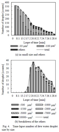
| 2017- 1. | Natsumi Yagi and Akira Kawai "Three-Dimensional Analysis of Liquid Propagation at Microchannel Junction using ESEM", J. Photopolymer Science and Technology, 30(6), 709-714 (2017) |
|
| [abstract] The three-dimensional wetting phenomena in a T-shaped microchannel made of a SU-8 photoresist accompanying with a pillar sub-pattern are analyzed by using an environmental scanning electron microscopy (ESEM). By lowering the sample temperature in the ESEM chamber at constant the H2O pressure, the water condensation occurs under H2O dew point and the liquid propagation in the microchannel can be observed. The experimental results show that the pinning angle of water flow at T-junction is 58 degrees in the T-shaped microchannel. In the case of the T-shaped microchannel with the sub-pattern, it is found that the pinning angle becomes low by adhering the water around the sub-pattern. These results can realize to the smooth flow at the channel junction without any water trapping for the three-dimensional microfluidic devices. Keywords: ESEM, Microchannel, Pillar-pattern, Three-dimensional analysis |
||
 |
 |
|
| 2017- 2. | Katsuaki Yamane and Akira Kawai "Application to Artificial Skin of Double Cone Tube Made of Acrylic Resin Formed by Micro Stereolithography" J. Photopolymer Science and Technology, 30(3), 345-350 (2017) |
|
| [abstract] A functional double cone tube (DCT) array with gas trapping and high durability is developed in the application of artificial skin. A stereo-lithography system is employed to fabricate DCT made of acrylic resin. In an aqueous solution, a certain amount of gas can be trapped in the tube due to capillary force balance. Under applying an external load, internal stress is effectively released at the interface between top and base cones. In the tactile sensing investigation, softness and tackiness senses as an artificial skin are felt. Keywords: Artificial skin, Micro stereo-lithography, Acrylic resin, Double cone tube (DCT), Gas storage, Stress distribution |
||
 |
 |
|
2016年 3報
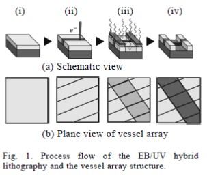
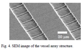
| 2016- 1. | Hiroki Nakano, Kenta Takahashi, Akira Kawai, "Negative Pattern Formation in Positive Resist Layer by EB / UV Hybrid Lithographys", J. Photopolymer Science and Technology, 29(4), 603-606 (2016) in perss. |
|
| [abstract] By the combination of EB (electron beam) pattern irradiation and UV (ultraviolet) exposure processes, negative tone pattern can be formed in a positive type resist film. It is well known that a novolac resin based resist film can be crosslinked by thermal and EB irradiation processes. By changing the EB irradiation and UV light exposure doses, a dissolution resistance of the resist film to TMAH (tetramethylammoniumhydroxide) alkaline aqueous solution can be controlled. As the result, the EB/UV hybrid lithography is effective for the fabrication of difference height patterns in a single resist layer. A dose response characteristic of a resist film is determined. A roughness of resist pattern in EB/UV hybrid lithography is also discussed. As an application, a micro square vessel array is fabricated used for a bioelec tronic field Keywords: electron beam lithography, photolithography, photoresist, atomic force microscopy (AFM), surface roughness, EB/UV hybrid lithography |
||
 |
 |
|
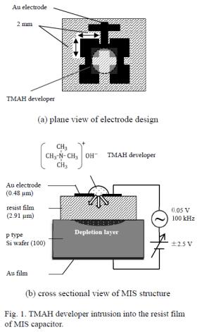
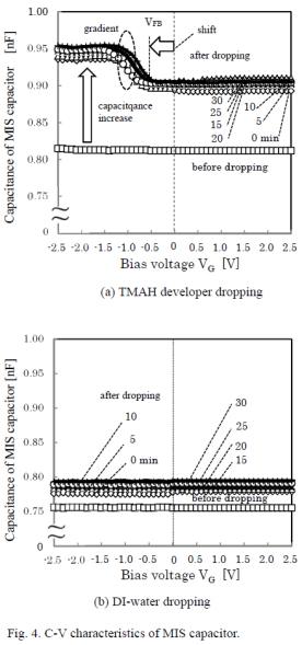
| 2016- 2. | Hodaka Shirataki, Akira Kawai, "In-situ Monitoring of TMAH Developer Intrusion into Resist Film by C-V Method", J. Photopolymer Science and Technology, 29(6), 817-822 (2016) |
|
| [abstract] The TMAH developer (2.38 wt% aqueous solution) intrusion into a resist film is analyzed by the typical current-voltage (C-V) method. As well known device structure, Metal / Insulator / Semiconductor (MIS) structure is employed, and a resist film (novolak resin base) is adopted to an insulator material. During the TMAH developer dropping on the Au mesh electrode, an increase of the capacitance and a parallel shift towards a negative gate bias voltage region in a C-V curve can be clearly observed. At the first stage of dropping, these signal changes in C-V curve are relatively large. Refractive index of the resist film slightly increases after the TMAH developer dropping, which reflects the condensation of polymer resin due to the TMAH developer intrusion. A contact angle decrease of the TMAH developer after dropping is also monitored. A spreading coefficient cS of TMAH developer decreases gradually as the time elapse. Particularly, the capacitance change clearly indicates the intrusion of the TMAH developer as the function of a time elapses. These dynamic measurements of the intrusion will be effective to analyze the liquid intrusion mechanisms into polymer materials. Keywords: liquid intrusion, TMAH developer, photoresist, MIS structure, C-V curve, dielectric constant, refractive index, contact angle, spreading coefficient, in-situ monitoring |
||
 |
 |
|
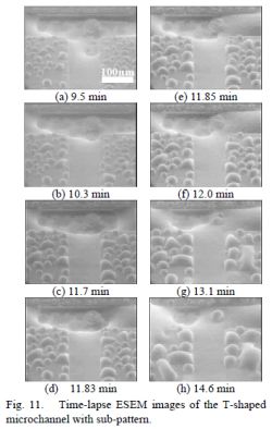
| 2016- 3. | Natsumi Yagi, Akira Kawai, "Effect of Sub-Pattern on Guiding Liquid Propagation at Microchannel Junction", J. Photopolymer Science and Technology, 29(6), 833-834 (2016) |
|
| [abstract] Keywords: sub-pattern, ESEM, microchannel, liquid flow, Young-Laplace equation, pinning effect |
||
 |
||
 |
 |
|
2014年 2報
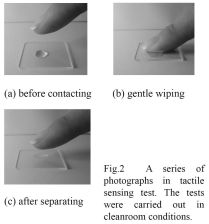
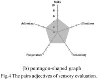
| 2014- 1. | Yako Kunii, Akira Kawai "Tactile senses control by contacting a human finger with micro resist pattern arrangements" J. Photopolym. Sci. Technol., 27 (6) 691-694 (2014) |
|
| [abstract] A functional micro resists structures with tactile characters of the human are developed due to sweat, sebum and water influence. A new method of tactilesensory evaluation with the pentagon-shaped graph is employed. It is found that the micro pattern acts to wet and to feel smooth and comfortable by immersing some kinds of liquids. By the surface energy analysis, the tactile sensory evaluation can be explained at the point of wetting nature. Keywords : human tactile sensitivity, lithography, micro pattern array, touch panel plate |
||
 |
 |
|
 |
 |
|
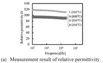
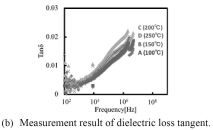
| 2014- 2. | Akira Kawai, Shogo Ohtani "Frequencydispersion of permittivity of SU-8 resist thin film" J. Photopolym. Sci. Technol., 27 (6) 711-712 (2014) |
|
| [abstract] Permittivity of a SU-8 (3050) resist film baked at 100, 150, 200 and 250℃ is characterized by a typical capacitance method in the frequency range from 100Hz to 5MHz. The permittivity is relatively constant in the frequency range, but slight dependency on baking temperature can be confirmed. The dielectric loss tangent of resist film increases gradually up to 0.03 but relatively low. The typical dielectric properties of resist material can be confirmed experimentally, which indicates an application possibility of resist material as an electronic device component material. Keywords: photoresist, SU-8, permittivity, dielectric loss, frequency response |
||
 |
 |
|
 |
||
2013年 7報
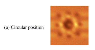
| 2013- 1. | Akira Kawai “Electrification on Condensation Surface of Micro Particles with Atomic Force Microscope (AFM)” J. Photopolymer Science and Technology, 26(6), 705-706 (2013). |
|
| [abstract] Keyword : atomic force microscope, micro particle, polystyrene latex, electrified image |
||
 |
 |
|
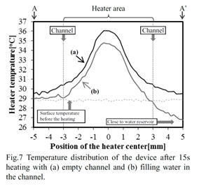
| 2013- 2. | Yuta Noguchi, Akira Kawai “Local Heating System Integrated with Platinum Micro Heater and Photopolymer Microfluidic Channel” J. Photopolymer Science and Technology, 26(6), 713-716 (2013). |
|
| [abstract] Local heating system composed with micro heater and microfluidic channel is designed and fabricated. Micro heater made of platinum film is formed on a slide glass by radio-frequency magnetron sputtering and lift-off processes. Microfluidic channel is designed to surround the micro heater. A SU-8 epoxy-based negative photoresist is employed as micro channel material and patterned by lithography process. The micro heater has ability to heat over 350℃at an electric power of 3.12W. Local heating property is evaluated by applying DC electric power. Heating area decreases 61.5% for micro channel filled with water by comparison with empty channel. Temperature of water in the micro channel is rise up 3.5℃ and heat absorption, which is estimated about 275.3μJ. The microfluidic channel with water is an effective method for local hearing. The local heating system with integration of micro heater and channel is one candidate which can apply to various fields such as biological and biomedical tools. Keywords : local heating system, micro heater, microfluidic channel, SU-8 photoresist |
||
 |
 |
|
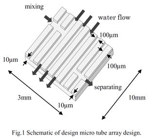
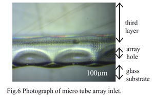
| 2013- 3. | Kazutoshi Otsuka, Kenta Takahashi, Akira Kawai “Fabrication of Micro Tube Array by Combining Positive with Negative Type Photoresists due to Solubility Difference in Developer” J. Photopolymer Science and Technology, 26(6), 717-720 (2013). |
|
| [abstract] The micro tube array in triple layer structure is constructed due to solubility difference phenomena. The triple layers are fabricated by photolithography process with i-line and SU-8 photoresists. The first and third layers are formed with SU-8 photoresist process. The second layer is formed by i-line photoresist process. Both i-line photoresist and unexposed SU-8 photoresist can be dissolved by dipping in the SU-8 developer at the same time. The exposed region of the SU-8 photoresist film is remained. The SU-8 photoresist film is formed in micro tube array structure. The shape of micro tube array is fabricated in rectangle of 10.0mm length and 3.05mm width. The array hole is formed 103μm width and 8.96μm thickness. By applying this process, unique structures of microfluidic system such as artificial capillary blood tube can be realized. Keywords : photoresist, solubility difference, capillary tube, micro tube, array structure, SU-8 photoresist |
||
 |
 |
|
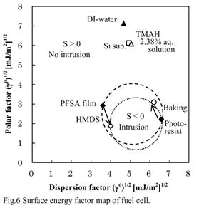
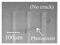
| 2013- 4. | Yosuke Sakurai, Kenta Takahashi, Akira Kawai “Liquid Penetration Control of Photoresist/Perfluorosulfonic Acid (PFSA) Double Layer Structure by Hydrophobic Treatment” J. Photopolymer Science and Technology, 26(6), 727-732 (2013). |
|
| [abstract] Silicon-based micro fuel cells are considerable interest for micro electromechanical system (MEMS) devices. Micro pattern fabrication by photolithography and etching process is effective for minimization of fuel cells. It is known that the photolithography process is difficult to employ for an electrolyte of perfluorosulfonic acid (PFSA) film due to swelling and peeling under wet process. In order to prevent the problems, a hexamethyldisilazane (HMDS) primer treatment is employed on the interface of photoresist/PFSA. Consequently, photoresist/PFSA double layer structure can be formed on the Si substrate with no defect formation. The double layer structure is selectively etched by reactive ion etching (RIE) process with CF4 gas in order to fabricate the micro pattern of PFSA film. The effect of HMDS primer treatment is observed as a hydrophobic effect by an analysis of wetting energy. The PFSA film with HMDS primer treatment should prevent to penetrate the liquid into the PFSA film under wet process. Keywords: perfluorosulfonic acid (PFSA), photolithography, hexamethyldisilazane (HMDS), reactive ion etching (RIE), adhesion property |
||
 |
 |
|
 |
||
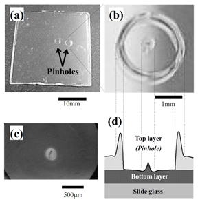
| 2013- 5. | Yuta Noguchi, Kenta Takahashi, Akira Kawai “Micro Pinhole Formation in Photoresist Multilayer Structure controlled with Hydrophilic Treatment” J. Photopolymer Science and Technology, 26(6), 739-744 (2013). |
|
| [abstract] The pinhole formation in photoresist multilayer structure acts as a critical defect for device fabrication. The purpose of this study is pinhole prevention by hydrophilic treatment and analysis of pinhole formation mechanism in terms of surface free energy. A SU-8 photoresist top layer is spin-coated on a SU-8 bottom layer as simplest multilayer structure. Pinholes are formed on bottom layer with no-treatment, however, pinholes cannot be observed when bottom layer is treated by hydrophilic process. Subsequently, the surface free energy and spread coefficients of each SU-8 layer are evaluated. Because the absolute value of spreading coefficient Stop is small relatively in case of no-treatment, the pinning phenomenon can be caused by contaminants. A triple point, bottom layer, liquid top layer and air, appears at the pinning area. Air cannot intrude into interface between top-bottom layers due to the spreading coefficient “Sair>0”. Consequently, the pinhole expansion phenomenon would be dominated by tensional force and viscous-elasticity of liquid top layer. By hydrophilic treatment, surface free energy of bottom layer increases drastically, therefore the pinning phenomenon is prevented because of “Stop<<0”. Keywords: pinhole, pinning, SU-8 photoresist, multilayer structure, hydrophilic treatment, surface free energy, spreading coefficient |
||
  |
||
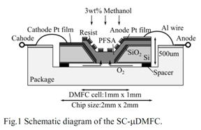
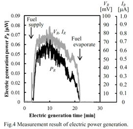
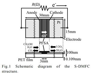
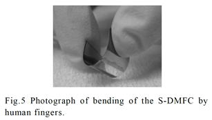
| 2013- 6. | Yosuke Sakurai, Daisuke Tanaka, Shunsuke Ohata, Akira Kawai “Fabrication and Durability of Single Chip Micro Direct Methanol Fuel Cell (SC-μDMFC) by Photolithography Process” J. Photopolymer Science and Technology, 26(6), 751-756 (2013). |
|
| [abstract] Single chip micro direct methanol fuel cell (SC-μDMFC) is attractive as a chip scale power source for micro electromechanical system (MEMS) devices. A multilayer structure is commonly employed for the fuel cell. The durability of SC-μDMFC should be mostly affected by interface energy. In this study, SC-μDMFC is fabricated by employing a photoresist / Pt electrode / PFSA film multilayer structure. The fabrication of SC-μDMFC (chip size of 2.0mm×2.0mm ×500μm) is succeeded without any film peeling. Consequently, maximum output power of 0.07μW is obtained. The film peeling of SC-μDMFC is also analyzed by the interface energy method. As a result, several layers of weak adhesion are predicted. However, the film peeling could not occur by the contribution of the other mechanical adhesion factors. The experimental results indicate the durability of the SC-μDMFC. Keywords : direct methanol fuel cell (DMFC), multilayer structure, photolithography, perfluorosulfonic acid (PFSA), adhesion property, spreading analysis |
||
 |
 |
|
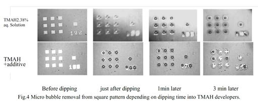
| 2013- 7. | Kenta Takahashi, Akira Kawai “Effect of Low Surface Tension Developer on Micro Bubble Removal from Resist Square Window Pattern” J. Photopolymer Science and Technology, 26(6), 765-768 (2013). |
|
| [abstract] In pattern developmemt, a removal property of bubbles formed on a concave window pattern made of DFR (dry film resist) is characterized. The sizes of the DFR window pattern are 100μm square and 50μm height. The fundamental factors of removal property can be explained by means of interaction analysis among interfacial energies. The experimental results obtained are analyzed based on the free energy balance model thermodynamically. The factor of micro bubble removal from the DFR window pattern is discussed for the suitable micro pattern fabrication. By adding a hydrophobic nonionic surfactant, both polar and dispersion components of surface energy of the developer clearly decrease. These components change act to decrease surface tension of the developer. The effectiveness of low surface tension developer on the removal property of micro bubble can be explained based on surface energy. Keywords : DFR, micro bubble, surface energy, window pattern, surfactant, TMAH developer |
||
 |
||
2012年 4報
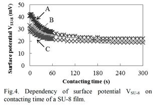
| 2012- 1. | Yuta Noguchi, Akira Kawai “Surface Stability of SU-8 film for Accurate Biopotential Detection” J. Photopolymer Science and Technology, 25(6), 719-722 (2012). |
|
| [abstract] Biopotential is important and sensitive information in order to monitor and control growth condition for living cells. For detecting biopotential change accurately, a stable biocompatible polymer film is required. In this study, a stable surface of a SU-8 film is characterized, and it is possible for applying to a cover material of electrode surface or an element of a biological implanted device. Surface potential VSU-8 of a SU-8 film is measured by making a metallic electrode contact. As a standard equilibrium, VSU-8 indicates exponential decreasing to reach at +21mV. Biopotential Vbio of plant cells indicates large potential change for 10 to 42mV range. This potential change means an individualistic signal of living cells. By combination of a SU-8 film and living cells, it is capable of obtaining accurate and effective data. Keywords : SU-8 resist, plant cells, surface potential, biopotential, biocompatible material |
||
 |
 |
|
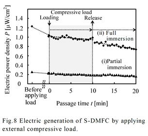
| 2012- 2. | Yosuke Sakurai, Akira Kawai “Mechanical Stress Effect on Ionic Conductivity of Perfluorosulfonic Acid (PFSA) Film by Photolithography” J. Photopolymer Science and Technology, 25(6), 723-727 (2012). |
|
| [abstract] Direct Methanol Fuel Cell (DMFC) consists of a perflurosulfonic acid (PFSA) electrolyte is attractive as a portable power source. It is possible to fabricate a DMFC array by dividing a PFSA film into micro pieces by photolithography. In this regard, it is known that photoresist film causes significant compressive and tensile stress generation in an underlying layer. Then it is needed to control preparation condition of photoresist film formed on a PFSA film. The effect of compressive load in a PFSA film is observed as enhancement of electro motive force. By applying compressive load to a PFSA film, proton ionic conductivity would be enhanced. On the other hand, a tensile load acts to decrease electro motive force. Therefore photoresist pattern shape should be designd effectively in order to enhance proton ionic conductivity of PFSA film. Keywords : stress, photoresist film, retention property, perflurosulfonic acid (PFSA), Direct Methanol Fuel Cell (DMFC) |
||
 |
 |
|
 |
||
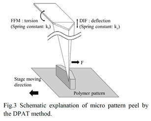
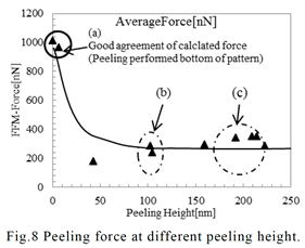
| 2012- 3. | Takashi Aiba, Akira Kawai “Micro Cantilever Motion in Micro Pattern Peeling by DPAT Method” J. Photopolymer Science and Technology, 25(6), 729-733 (2012). |
|
| [abstract] DPAT (Direct Peeling by using AFM tip) method provides direct measurement of a peeling force of micro-structure. A peeling force of micro polymer pattern at different peeling height is analyzed. When a cantilever is made a contact with a bottom of pattern, peeling force and displacement of cantilever are larger than in those of pattern top. The cantilever motion is analyzed peeling phenomena in different peel height. The peeling force of pattern is determined to around 1μN. The peeling force applying at pattern bottom reflects the adhesion force. The effectivity and accuracy of the DPAT method is discussed. Keyword : polymer micro pattern, atomic force microscope, direct peeling by using AFM tip (DPAT), adhesion force, cohesion failure, interface failure |
||
 |
 |
|
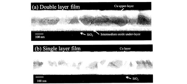
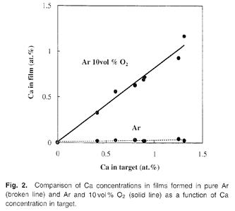
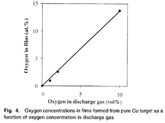
| 2012- 4. | Satoru Mori, Akira Kawai “Interfacial Microstructure of a Double-layer Cu Film Consisting of an Under-layer Deposited on SiO2 Substrate in Ar-10 vol% O2 and an Upper-layer Deposited in Pure Ar” J. Adhesion Soc. Japan, 48(1), 10-16 (2012). |
|
| [abstract] Interfacial microstructure of a double-layer Cu film, composed of an under-layer deposited on SiO2,in Ar-10voI% O2 followed by an upper layer deposited in pure Ar, was investigated for thin film conductor tracks for large and high-definition liquid crystal displays. The layer deposited in Ar-10vo1% O2 has fine-grain, and contains Cu and Cu2O. Detailed analysis shows the interface between the under-layer and SiO2 substrate isn't flat, but concavity and convexity. Addition of oxygen to the discharge gas generates Cu2O in the under-layer. Cu2O dissolves in the SiO2, and forms CuO-SiO2 eutectic. The dissolution of Cu2O in SiO2 must increase anchor effect and the adhesive strength. Keywords : copper, film, sputtering, oxygen, LCD |
||
 |
||
2011年 2報
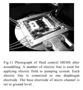
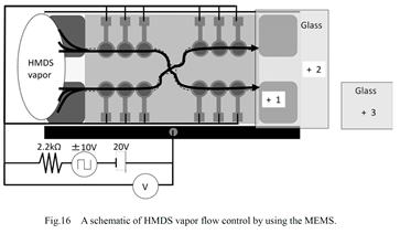
| 2011- 1. | Akira Kawai “Fluid Control MEMS constructed with Polymer Materials” J. Photopolymer Science and Technology, 24(5), 587-593 (2011). |
|
| [abstract] A polymer material indicates higher durability and resistance properties against to reactive gases,acid and alkaline solutions. Fluid control MEMS (micro electro mechanical systems) with micro diaphragm pumping system used for reactive gas control is constructed. A resist film made of novolac resin as a diaphragm material is employed. An Au/Si/resist multilayer structure as a diaphragm of 1mm diameter is formed by optical lithography and anisotropic wet etching techniques. A micro channel structure of 50μm width is also fabricated by employing a polymer thick film. The mechanical strength of a diaphragm is tested by applying static load using a probe system.By applying 20V bias between diaphragm and base electrodes,Coulomb attractive force acts to operate the diaphragm motion. As the fluid flow control, a silane-coupling vapor gas of HMDS (hexamethyldisilazane) is employed. A contact angle of water indicates hydrophobic of a glass substrate by HMDS vapor control using the MEMS. Keywords : MEMS, fluid control, novolac resist, HMDS, diaphragm, micro channel, contact angle, hydrophobic treatment |
||
 |
||
 |
||
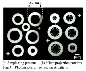
| 2011- 2. | Masayoshi Yamada, Akira Kawai “Micro Polymer Capsule Constructed with Micro Pillars Formed by Multi Laminating Method” J. Photopolymer Science and Technology, 24(6), 647-650 (2011). |
|
| [abstract] A micro polymer capsule of 6.5mm length and 4.0mm diameter is fabricated by multi laminating method. The micro polymer capsule has 56micro pillars for generating a turbulent liquid flow in the inside of capsule. As a fabrication process, the SU-8 resist film based on epoxy resin is coated on a glass substrate. A ring shape image is exposed on the resist film. After pattern development, the ring patterns are peeled from the glass substrate by dipping into HF aqueous solution. The SU-8 ring patterns are stacked in 18 layers by using the micro tweezers under the alignment accuracy of ±0.3mm. In order to adhere the SU-8 ring layers each other, an i-line resist material is pasted into SU-8 ring patterns, then baked on a hotplate at 200℃ for 10min. These functional capsule structures can contribute to develop various biological and medical MEMS (Micro Mechanical electronic system) devices. Keywords : micro polymer capsule, micro pillar, stacked structure, adhesion, MEMS, SU-8 resist |
||
 |
 |
|
2010年 6報
| 2010- 1. | Satoru Mori, Akira Kawai “Low-Resistivity and Adhesive Sputter-Deposited Cu-Ca Films with an Intermediate Oxide Layer” Jpn. J. Appl. Phys., 49 (2010) p075804-1~8. |
|
| [abstract] We investigated a method of producing low-resistivity and adhesive sputter-deposited copper alloy films with an intermediate oxide layer that retains its adhesion after hydrogen annealing for applications of electric interconnections for thin film circuits and liquid crystal displays. The formation of an intermediate copper oxide layer between a copper film and a substrate by sputter deposition in the presence of oxygen enhances adhesion. However, when such films are exposed to hydrogen at elevated temperatures, hydrogen penetrates the films and reduces copper oxide. This reaction generates water molecules, which aggregate at the interface between the copper film and the substrate. As a result, microvoids form at the interface, degrading the film adhesion. Sputter-deposited films with an intermediate oxide layer produced from a Cu-Ca target are adhesive even after hydrogen annealing. As films deposited in pure argon have low resistivities, it is possible to form low-resistivity and adhesive metallization. |
||
 |
 |
|
| 2010- 2. | Tetsuya Ono, Akira Kawai “Free fall Mechanism of Micro Liquid Droplet” J. Photopolymer Science and Technology, 23(3), 363-366 (2010). |
|
| [abstract] It is important to analyze a behavior of micro liquid droplet in order to achieve a high accuracy of LSI fabrication process such as the cleaning process, the lithography process and the etching process, patterning process and so on. By using a high-speed camera, free fall behavior of a droplet is observed. The Laplace force before falling acts to a droplet effectively. By observing the position of droplet head and tail, it is observed that the micro droplet falls faster than the free fail velocity. By employing a droplet spring vibration system, the fall nature can be clarified. Keywords : Micro droplet, Laplace, free fall, ink jet, surface tension |
||
 |
 |
|
| 2010- 3. | Masayoshi Yamada, Akira Kawai “Characterization of Resist Micro Pattern Adhesion by Applying Ultrasonic Vibration” J. Photopolymer Science and Technology, 23(3), 435-438 (2010). |
|
| [abstract] An improvement of resist pattern adhesion has been recognized as one important problem that needs to be solved in micro device fabrication. Dry film resist (DFR) patterns in circle shape are fabricated on glass substrates for the adhesion test. By applying ultrasonic vibration on a edge of DFR pattern in deionized (DI) water, the time until peeling occurred is measured. The DFR pattern can be peeled from a glass substrate under the ultrasonic vibration at 25kHz. The water intrusion model into the DFR/glass interface is employed in order to discuss the adhesion behavior. Keywords : dry film resist, ultrasonic vibration, peeling strength, surface energy, water intrusion |
||
 |
 |
|
| 2010- 4. | Shunsuke Ohata, Akira Kawai “Dielectric Property of Solution Analyzed by using pn-junction Array” J. Photopolymer Science and Technology, 23(3), 367-370 (2010). |
|
| [abstract] Drying property of water thin film formed on a pn-junction array substrate is characterized based on dielectric analysis. In wetting processes such as pattern development, wet etching wet cleaning and drying are recognized as important processes in order to fabricate high quality electronic devices. The pn-junction array is designed with a Combination of micro pattern networks. By using a FRA (Frequency Response Analyzer) system, the drying process of water thin film can be monitored. A rapid decrease of capacitance value is observed as vanishing the micro meniscus bridge. The application of endpoint detector of drying of water thin layer is discussed. Keywords : Pn-junction, dielectric property, FRA, water thin film, micro meniscus, Laplace force |
||
 |
 |
|
| 2010- 5. | Junji Miyazaki, Nobuhito Toyama, Akira Kawai “Double Patterning Analysis Method by Emulation using a Double-Exposure Technique” Jpn. J. Appl. Phys., 49 (2010) p035201-1~6. |
|
| [abstract] Double patterning lithography was utilized to break the resolution limit of lithography and is the most promising technology that enables shrinking of this limit. There are some barriers concerning evaluation of the double patterning process because it includes the hard mask fabrication and dry etching process. We proposed a new evaluation method for double patterning to analyze photomask performance with an easy are simple procedure using a double-exposure technique. Results showed this emulation method was useful in determining the impact of mask overlay and critical dimension (CD) error on double patterning lithography. We also evaluated the impact of mask overlay and CD. Both the overlay are CD difference were very good between the two masks. Correlations between mask and wafer cannot be detected because of the measured overlay error and the CD performance of masks was too small. |
||
 |
||
| 2010- 6. | 山田昌佳、河合 晃、大澤義征、宝泉俊寛 「超音波プローブ振動法によるはんだバンプの付着性解析」 Microjoining and Assembly Technology in Electronics (Mate), 93-98 (2010). |
|
| [abstract] The new adhesion reliability test of isolated for an isolated solder bump mounted on a glass epoxy substrate is demonstrated. The isolated solder bump can be peeled spontaneously from a glass-epoxy substrate by applying ultrasonic vibration at 25kHz on a top of solder bump. The applying time until peeling occurs is employed as a meaningful value for evaluating the adhesion reliability of solder bump. The peeling energy of solder bump can he also estimated from the vibration energy of the ultrasonic probe. The peeling energy of lead free(Sn-3.0Ag-0.5Cu) solder bump becomes high (292.4±31.1 kJ/m2) as compared with that (134.7±31.1 kJ/m2) of eutectic(Ph-63Sn)solder bump. The validity of this method is discussed. Keywords : BGA(Ball Grid Array), Ultrasonic vibration. Adhesion reliability, Interface peeling |
||
 |
 |
|
2009年 5報
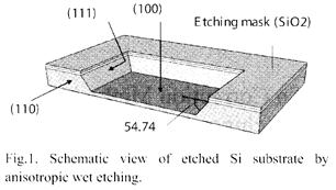
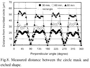
| 2009- 1. | Junji Miyazaki, Akira Kawai “Fidelity of Mask Shape and Use of a Correction Method in Anisotropic Si Wet Etching” J. Photopolymer Science and Technology, 22(6), 731-735 (2009). |
|
| [abstract] Anisotropic wet etching is widely used in MEMS fabrication processes. As this etching has different etching rates for each crystal lattice face, the etched window shape changes during etching. The fidelity of the mask shape is discussed and a correction method is proposed. It was shown that a rectangle tilted 45 degrees to (110) became octagonal and finally rectangular in shape parallel to (110), while a rectangle parallel to (110) maintained its shape. A circle mask shape also became octagonal and then rectangular. It was demonstrated that deviations from the designed shape that occur during the etching can be corrected on the mask shape in advance. This method is useful for the fabrication of circular etched window shapes. Keywords: Anisotropic etching, MEMS, Si wafer, mask, correction |
||
 |
 |
|
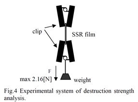
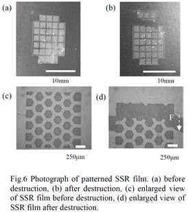
| 2009- 2. | Akihiro Takano, Akira Kawai “Analysis of self-standing structure composed by thick resist layer” J. Photopolymer Science and Technology, 22(5), 561-564 (2009). |
|
| [abstract] A self-standing resist (SSR) film in hexagonal lattice structure is fabricated and tested its destruction strength. The resist film formed on a glass substrate is removed from the glass substrate by wet etching. As a result, higher destruction strength of the SSR film with micro-hexagonal hole array can be obtained compared with that without holes. Keywords : self-standing structure, hexagonal lattice structure, photoresist,destruction strength, MEMS |
||
 |
 |
|
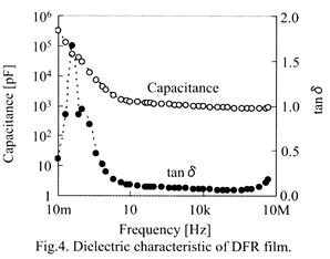
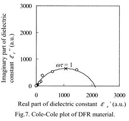
| 2009- 3. | Hiroki Sasazaki, Akira Kawai “Dielectric dispersion analysis of resist layer” J. Photopolymer Science and Technology, 22(3), 317-320 (2009). |
|
| [abstract] Dielectric properties of resist materials such as dielectric frequency dispersion,permittivity and dielectric loss tangent,which should be optimized in structural material designing, are characterized. Dielectric properties of resist materials are characterized by traditional capacitance method in the frequency range of 10mH to 5MHz. The relative dielectric constant and loss tangent from dry film resist (DFR) at 1MHz can be determined to be 3. 63 and 0.0744. The Cole-Cole plot is employed to determine a dielectric relaxation time of dipole moment in polymer structure. The relaxation time of DFR film can be determined to be 12.1s. The validity of dielectric properties of DFR film as a structural material is discussed. Keywords : dielectric constant, frequency dispersion, dielectric relaxation time, MEMS |
||
 |
 |
|
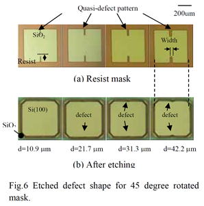
| 2009- 4. | Junji Miyazaki, Akira Kawai “Formation Mechanism of Micro Defect in Anisotropic Etching Analyzed by using Quasi-defect Pattern” J. Photopolymer Science and Technology, 22(3), 313-316 (2009). |
|
| [abstract] Anisotropic wet etching for Si substrate is a key technology for manufacturing three dimensional structures for MEMS. It is important to understand a printability of defect during this etching process to create a complete design of MEMS structure. In this paper, an impact of quasi-defects on an etched structure is investigated. It is demonstrated that a minimum defect size which is not affect on the final structure is around a half of total etching depth. Keywords : Anisotropic etching, defect, photo lithography, MEMS, Si wafer |
||
 |
||
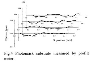
| 2009- 5. | Junji Miyazaki, Akira Kawai “Characterization of photomask substrate in optical lithography” J. Photopolymer Science and Technology, 22(5), 555-559 (2009). |
|
| [abstract] The characteristic of a photomask strongly impacts lithography performance since it is part of the optical system. In this paper, we investigate characteristics of photomask substrate flatness impact on optical lithography. It is demonstrated that high and mid spatial frequencies of substrate flatness variation are too small enough to affect lithographic performance. However, a low spatial frequency of flatness variation could cause a focal plane deviation. We show that the flatness of exposure area after tilt and curvature correction directly corresponds to an image plane deviation. Keywords : photomask, flatness, focus, lithography, AFM |
||
 |
||
2008年 11報
| 2008- 1. | Daisuke Tanaka, Akira Kawai “Flowing control of micro bubbles in DFR micro fluidic channel formed on metal /insulator composite substrate” J. Photopolymer Science and Technology, 21(1), 63-68 (2008). |
|
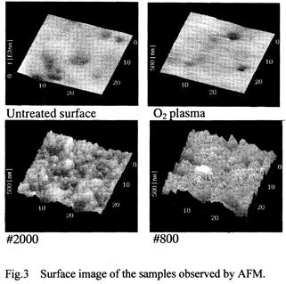
| [abstract] Dry film resist (DFR) and thick resist by spin coat (TRS) provide well-defined resist profiles with high aspect ratio, and they are also suitable for use as a permanent resist material. These resists have been widely used in the micro fluidic (inkjet, reactor, biochip) fields. The flowing control of micro bubbles is carried out in the permanent resist micro fluidic channel formed on the metal/insulator composite substrate. As the result, these micro bubbles were more likely to trap at the Au surface by controlling the surface free energy of DI-water. Furthermore, in order to prevent the bubble formation in the channel, it is effective to control the surface free energy. The O2 plasma treatment is also effective to prevent the bubble trapping. Keywords : dry film resist, thick resist by spin coat, micro channel, micro bubble, surface energy |
||
 |
||
| 2008- 2. | Akira Kawai, Daisuke Tanaka, Sachito Matsubara, Masayoshi Ogata, Kazutoshi Tachibana “Wetting control of polymer solution on roughened solid surfaces by wet-blast technique” J. Photopolymer Science and Technology, 21(1), 37-42 (2008). |
|
| [abstract] Spreading of organic solution can be improved drastically on a solid surface after the wet-blast treatment. The wet-blast treatment has an ability of morphology control of various kinds of surfaces. Various organic liquid can spread spontaneously on a substrate due to spreading energy S. By analyzing surface energies of the treated surfaces, the wet-blast treatment has a similar effect of the increase of dispersion component γd , that is, hydrophobic surface. Spontaneous spreading of the polymer solutions can be explained to be negative value of the spreading coefficient. High wetting surface can be realized by an oxygen plasma treatment. However, the substrate surfaces become considerable hydrophilic property due to increase of the polar component γp , that is, hydrophilic surface. It can be considered that water vapor adsorbed the hydrophilic substrate and induce corrosion of metal components such as an electrode and micro wire lines. The roughened surface can act to prevent liquid condensation after spreading on the substrate, so-called "pinning effect". The spontaneous spreading on the substrate after wet-blast treatment can be explained on the multiplier effect of nominal dispersion increase and pinning. Keywords : wet-blast technique, surface treatment, surface roughness, surface energy, spreading coefficient, pinning effect, resist solution, epoxy solution, dispersion component, polar component, oxygen treatment, hydrophilic property. |
||
 |
||
| 2008- 3. | Akira Kawai, Daisuke Tanaka, Tomotaka Ariga “Micro channel device composed by Dry film resist” J. Photopolymer Science and Technology, 21(1), 43-46 (2008). |
|
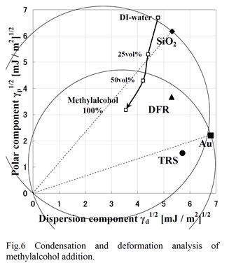
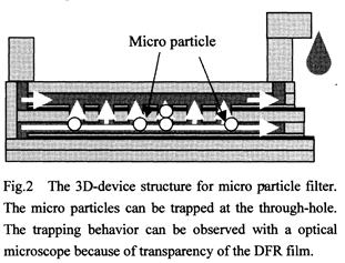
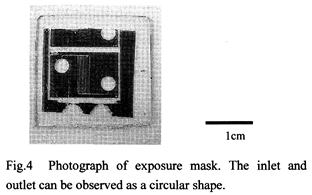
| [abstract] Micro particles path through in a concave channel and are trapped at a through hole in the filter structure. In the experiments, the deionized (DI) water is dropped on a micro 3D-filtering system constructed by a dry film resist (DFR) pattern. The filtering system is composed by an inlet hole of micro liquid drop, a micro channel, a micro filter and an outlet channel. In the result, the micro particles condensed and trapped at the different position in various shape patterns. The flowing and trapping of micro particles in a micro filtering device has been recognized as one important factor in functional micro device manufacturing. The construction of 3D-structure under acting Laplace force is accomplished without the structure destruction. The force acting on the micro particles and DFR structure is controlled by adjusting surface energy of methanol solution. We can control and predict the micro filtering system by designing micro pattern arrangement. Keywords : micro channel, liquid mixer, micro filter, 3D-structure, dry film resist, lithography, micro particle, Laplace force |
||
 |
 |
|
| 2008- 4. | Akira Kawai, Takashi Yamaji, Hiroshi Horiguchi “Adsorption of micro tip on various surface energy substrates” J. Photopolymer Science and Technology, 21(1), 85-88 (2008). |
|
| [abstract] Interaction in liquid medium has been focused for analyzing pattern development, pattern plating, wet etching and cleaning. Adsorption forces due to surface energy of a micro tip and various inorganic substrates can be measured in liquid environment. Hamaker constant between two surfaces is determined based on Lifshitz theory. In liquid condition, Hamaker constant in this system is proportional to adhesion force between the tip and substrates. Experimental value of Hamaker constant indicates good agreement with that of theoretical one. Keywords : interaction, Hamaker constant, surface energy, atomic force microscope,adhesion |
||
 |
 |
|
| 2008- 5. | Takashi Yamaji, Akira Kawai “Non-contact deformation of resist micro pattern due to van der Waals Interaction” J. Photopolymer Science and Technology, 21(1), 89-94 (2008). |
|
| [abstract] Deformation and stress distribution of ultra thin resist pattern are estimated by finite element method (FEM) from the measurement values of van der Waals (vdW) force and mechanical properties of resist material. In this simulation, strain and stress distribution in the simple model of the resist pattern are obtained. These results show that the thin resist pattern has high sensitivity to weak vdW force. And, the stress concentrates at an interface between the resist pattern and the substrate. The stress concentration point in the resist pattern would be destructed due to the weak force. In the experiment, the vdW attractive force is measured with an atomic force microscope (AFM) system. The maximum value of the attractive force is about 180nN. The error of the force measurement is prevented to be lower because the no torsion of the cantilever can be observed when the tip is approaching to the thin film resist surface. It is possible to discuss the realization of a soft micro chamber wall made of a soft material such as the cell. Keywords : resist pattern, non-contacting deformation, stress concentration, van der Waals force, atomic force microscope |
||
 |
 |
|
| 2008- 6. | Akira Kawai, Masahito Hirano and Takashi Yamaji “Nano-scale Deformation of Resist Film Surface by Humidifying and Drying Processes” J. Photopolymer Sci. Technol., 21(6), 737-738 (2008). |
|
| [abstract] Nano-scale deformation of resist film surface is analyzed by using atomic force microscope (AFM) in a humidity controlled chamber. It is clarified that the condensation size of polymer aggregates of resist material are slightly changed due to humidity change. As one major factor, Laplace force acting among polymer aggregate due to surface adsorbed water is discussed. The deformation model of condensed polymer aggregates is proposed. Keywords : resist pattern, deformation, polymer surface, water meniscus, adsorbed water, atomic force microscope |
||
 |
||
| 2008- 7. | Akira Kawai, Daisuke Tanaka “Micro Bubble Removal Depending on Glass Cleanness” J. Photopolymer Sci. Technol., 21(6), 727-728 (2008). |
|
| [abstract] One serious problem for immersion lithography is micro bubble adhesion which is responsible for various exposure failures. In immersion lithography, it seems reasonable to suppose that organic contamination of lens surface brings about micro bubble adhesion onto them. Therefore, this study is intended as an analysis of adhesion and removal of micro bubbles on quartz surfaces by the contact angle method. We discuss the adhesion and removal behavior of micro bubble on the point of the balance model of surface energy. In the consequence, the micro bubbles are more likely to adhere to the organic contaminate on the quartz substrate. Keeping cleanness of a lens surface is necessary in order to prevent the micro bubble adhesion. Keywords: immersion lithography, micro bubble, removal, adhesion, surface energy |
||
 |
 |
|
| 2008- 8. | Akira Kawai, Takashi Yamaji “Internal Stress of Dry Film Resist in Multilayer Structure” J. Photopolymer Sci. Technol., 21(6), 725-726 (2008). |
|
| [abstract] Multilayer resist process has been recognized as one candidate to realize high aspect ratio resist pattern. As one important control factor, strain and stress matching in multilayer structure should be taken into consideration. By using a strain gauge, the strain of dry film resist (DFR) in single, double and triple layer structure are measured as a function exposing time. The strain of DFR increases in proportion with the exposure dose but slightly decrease as number of multilayer. The stability of DFR multilayer structure is discussed. Keywords : multilayer structure, DFR, strain, internal stress, strain gauge |
||
 |
||
| 2008- 9. | Akira Kawai, Junko Kawakami, Hiroki Sasazaki “Surface Energy change of Si(100) Wafer by Exposing to Air” J. Photopolymer Sci. Technol., 21(6), 739-740 (2008). |
|
| [abstract] By contact angle method, surface energy of Si (100) wafer is measured with lapse of time in ambient condition. The polar component γsp of surface energy increases drastically but the dispersion componentγsd decreases. Surface energy γ(=γsd+γsp) gradually decreases. The surface energy change is mainly reflected with native oxide growth on the Si substrate. The polar and dispersion component of resist film corresponds mostly to those of surface energy of Si (100) after 10h exposing time to air. The spin coating condition can be designed effectively base on the surface energy model. Keywords : native oxide, surface energy, dispersion component, polar component |
||
 |
||
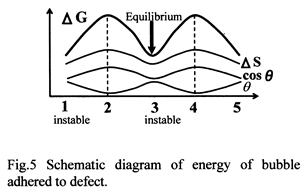
| 2008-10. | Akira Kawai, Hotaka Endo and Daisuke Tanaka “Pinning Effect of Micro Bubbles adhered on Resist Substrate” J. Photopolymer Sci. Technol., 21(6), 753-754 (2008). |
|
| [abstract] We discuss adhesion and removal properties of micro bubbles based on thermodynamics. It is important to consider the remove technique of micro bubbles from resist surface. A micro defect on a resist surface acts to enhance the adhesion of micro bubble on to them. It is cleared that the defect such as a solid particle and a resist fragment are more likely to capture the micro bubbles due to pinning effect. It is clarified that the removal mechanism can be explained based on surface energy balance model. Consequently, one can safely state that the removal of micro bubble from the F2 excimer resist film is required a certain external load. The capture mechanism of micro bubbles at the micro defect is analyzed based on the pinning effect. Keywords : excimer resist, micro bubble, pinning effect, surface energy, adhesion, defect |
||
 |
 |
|
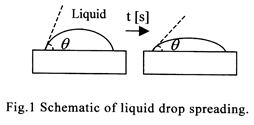
| 2008-11. | Akira Kawai, Akihiro Takano “Spreading of Liquid Drop on Resist Film Surface” J. Photopolymer Sci. Technol., 21(6), 759-760 (2008). |
|
| [abstract] Liquid drop spreading is effective phenomenon for understanding nature of wetting processes such as pattern development, etching, cleaning, immersion lithography and so on. Liquid spreading can be measured by contact angle measurement. Spreading coefficient c in Neumann model is estimated for each film surface. Results obtained in this experiment indicate that the liquid drops on resist surfaces are more likely to spread compared with those on the inorganic substrates. Keywords : resist, contact angle, Neumann spreading model, spreading coefficient |
||
 |
 |
|
2007年 12報
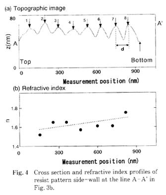
| 2007- 1. | 河合 晃、川上喜章 「原子間力顕微鏡(AFM)による微細レジストパターン内の屈折率分布の解析」 日本接着学会誌、vol.43, No.4, 140-143 (2007). |
|
| [abstract] 光リソグラフィー技術により作製したレジストパターンの側面には, 110~180nm程度の周期の波形模様が形成される。この波形模様は,パターン露光時の定在波効果に起囚して形成される。原子問力顕微鏡(atomic force microscope: AFM)を用いて, 直径0.61μm, 高さ1.03μmの円筒形レジストパターンを基板上で剥離倒壊させて, パターン側面に形成された波形模様を観察した。波形模様の周期はパターン側面内で異なることより, レジストパターンの高さ方向の屈折率分布を求めた。その結果, 屈折率は1.51~1.79の範囲で, パターン上部から底部へ向けて徐々に高くなっていることが分かった。これは, ホットプレートを用いた熱処理により, レジストパターン底部の凝集性が高くなったことを反映していると考えられる。この手法により, 微小固体内の光学パラメータおよび凝集性を解析することが可能になる。 By optical lithography, a wave shape is formed on a side wall of a column type resist pattern due to standing wave effect which occurs during exposure process. After the pattern collapse with atomic force microscope (AFM) , surface topography of the pattern side-wall can be imaged clearly. Based on standing wave effect, refractive index distribution of the resist pattern can be estimated to be the range from 1.51 to 1.79. It is clarified that refractive index at the pattern bottom is relatively high comparing, with that of the pattern top. This tendency reflects the distribution of cohesion strength of the resist pattern resulting from the heat treatment with a hot plate. By this method, optical and cohesion properties of a micro condensed matter can be analyzed quantitatively. |
||
 |
 |
|
| 2007- 2. | Akira Kawai, Kenta Suzuki “Bubbles Condensed at Water/resist Interface Analyzed by Atomic Force Microscopy” J. Photopolymer Science and Technology, 20(5), 673-678 (2007). |
|
| [abstract] Interaction acting between a micro tip and a micro bubble formed on a thin film surface of ArF excimer resist can be analyzed quantitatively by using atomic force microscope (AFM). The semi-sphere area of the observed bubble is approximately 25 μm diameter and 0.72 μm height. By approaching the AFM tip onto the bubbles in deionizad water, repulsive and attractive forces can be detected. These phenomena can be discussed on the basis of Laplace pressure. The AFM tip is more likely to indent into the bubbles compared with the resist film. The indentation analysis of the AFM tip is effective in order to identify the bubbles and to distinguish from other solid particles. Keywords : bubble, ArF resist, atomic force microscope, interaction force, tip indentation, Hamaker constant, immersion lithography |
||
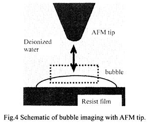 |
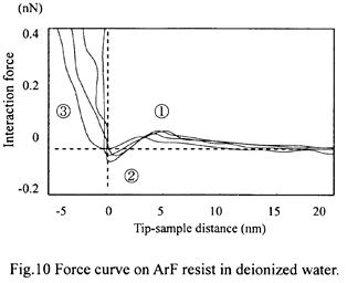 |
|
| 2007- 3. | Akira Kawai, Norio Moriike “Visualization of stress distribution in resist film by surface plasma treatment” J. Photopolymer Science and Technology, 20(6), 783-784 (2007). |
|
| [abstract] Keywords : polymer, crack, stress, finite element method, plasma, strain, stress release pattern |
||
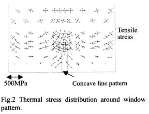 |
||
| 2007- 4. | Masaki Yamanaka, Akira Kawai “Analysis of micro meniscus shape by light scattering” J. Photopolymer Science and Technology, 20(6), 781-782 (2007). |
|
| [abstract] It is important to analyze a micro meniscus shape formed at a small nozzle apex in order to optimize a dispense performance in liquid spin coating. A meniscus bridge of deionized (DI) water is formed at a small gap between two nozzles and its curvature radius is changed due to water evaporation. When the incident light enters the meniscus bridge, the light is scattered depending on the meniscus shape. By monitoring the permitted light intensity passed through the meniscus bridge, the formation and vanishing mechanisms of the meniscus bridge can be discussed. Keywords : water meniscus, nozzle, light scattering, coating, evaporation, resist |
||
 |
||
| 2007- 5. | Akira Kawai, Takahiro Moriuchi “Non-contacting deformation (NCD) of line resist pattern due to interaction force with AFM tip” J. Photopolymer Science and Technology, 20(6), 777-780 (2007). |
|
| [abstract] It is entirely fair to say that the minute resist pattern should be deformed due to interaction force without any contact force, that is, non-contacting deformation (NCD). The NCD of a resist pattern can be analyzed based on the interaction investigation using atomic force microscope (AFM). An EB chemically amplified line resist patterns from 60 to 115 nm width and 210 nm height were used as the test patterns. In the force measurement, the AFM tip approaches to the top corner of line resist pattern, then, the AFM tip begins to bend toward the resist pattern due to the interaction force. We calculated the amount of NCD of the line resist pattern by 3D-finite element method (FEM). As decreasing the resist pattern width, the interaction force decreases but the NCD of resist pattern increases. The NCD less than 50nm design rule is also discussed quantitatively. Keywords : non-contacting deformation (NCD), interaction force, resist, Hamaker constant, atomic force microscope, finite element method (FEM) |
||
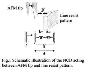 |
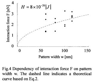 |
|
| 2007- 6. | Kenta Suzuki, Akira Kawai “Micro bubbles formed on ArF excimer resist surface detected by tip scanning method” J. Photopolymer Science and Technology, 20(6), 805-806 (2007). |
|
| [abstract] Keywords : micro bubble, atomic force microscope, defects, immersion lithography |
||
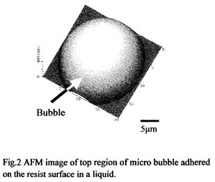 |
||
| 2007- 7. | Akira Kawai, Junko Kawakami “Wetting analysis of hydrophobic substrate treated by HMDS primer” J. Photopolymer Science and Technology, 20(6), 815-816 (2007). |
|
| [abstract] Keywords : HMDS, primer, contact angle, hydrophobic, wetting, adhesion |
||
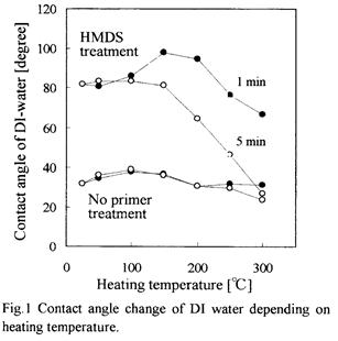 |
||
| 2007- 8. | Akira Kawai, Masahito Hirano “Nano-wetting of DI-water analyzed by AFM” J. Photopolymer Science and Technology, 20(6), 813-814 (2007). |
|
| [abstract] Keywords : liquid drop, surface energy, contact angle, atomic force microscope, size effect, mica surface |
||
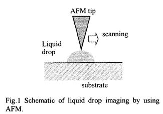 |
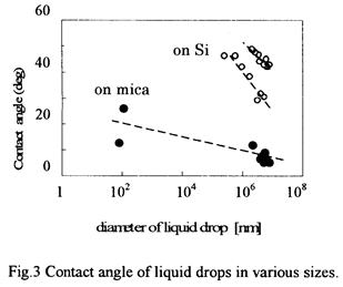 |
|
| 2007- 9. | Shingo Kuroda, Tomohiro Goto, Osamu Tamada, Masakazu Sanada, Akira Kawai “Analysis of interface condition between BARC and resist film by FT-IR/ATR” J. Photopolymer Science and Technology, 20(6), 807-808 (2007). |
|
| [abstract] Adhesion property of an ArF resist pattern formed on bottom anti-reflection coating (BARC) is considered to be sensitive to its interface condition. We examine the interface properties by Fourier transform infrared spectroscopy (FT-IR) attenuated total reflection (ATR) technique. As a result, a sample which was treated with a primer such as HMDS mixture indicates specific spectrums. This result gives an important suggestion that an intermediate layer between the BARC layer and the ArF resist would be formed by the primer treatment. This intermediate layer would act as a factor of the adhesion property. Keyword: BARC, primer, resist, ArF, Intermediate layer, FT-IR, ATR, HMDS |
||
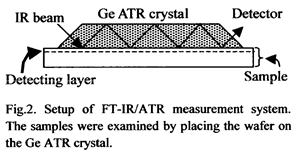 |
 |
|
| 2007-10. | Kazutoshi Kurano, Takahiro Kishioka, Yoshiomi Hiroi, Takuya Ohashi, Akira Kawai “Peeling analysis of ArF resist pattern on BARC by using AFM” J. Photopolymer Science and Technology, 20(6), 825-826 (2007). |
|
| [abstract] Keyword: BARC, atomic force microscopy (AFM), pattern collapse, direct peeling method with AFM Tip (DPAT) |
||
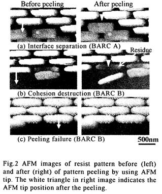 |
||
| 2007-11. | Kazutoshi Kurano, Takahiro Kishioka, Yoshiomi Hiroi, Takuya Ohashi, Akira Kawai “Deformation analysis of ArF resist pattern by using AFM” J. Photopolymer Science and Technology, 20(6), 827-828 (2007). |
|
| [abstract] Keyword: BARC, atomic force microscopy (AFM), pattern collapse, direct peeling method with AFM Tip (DPAT) |
||
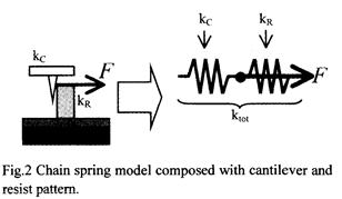 |
 |
|
| 2007-12. | Harumitsu Kubota, Akira Kawai “Native oxide growth on Si(100) surface in liquid environment” J. Photopolymer Science and Technology, 20(6), 823-824 (2007). |
|
| [abstract] A native oxide layer on a silicon substrate has an effect on adhesion of a resist micro pattern. Native oxide growth is investigated in various environments such as air, DI(deionized)-water and methanol. In air and DI-water, the native oxide thickness increases gradually as the storage time increases. On the other hand, in methanol, the growth rate of native oxide is quite low for the storage of 5h. In order to obtain a stable surface condition of Si substrate, these results can be applied effectively. Keyword : native oxide, storage, methanol, surface treatment, lithography |
||
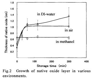 |
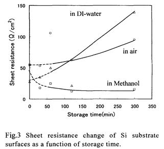 |
|
2006年 8報
| 2006- 1. | Akira Kawai, Takahiro Moriuchi, Takayoshi Niiyama, Takahiro Kishioka, Daisuke Maruyama,
Yasushi Sakaida, Takashi Matsumoto “Adhesion improvement of ArF resist pattern depending on BARC material” Microelectronic Engineering, 83, 659-662 (2006). |
|
| [abstract] The improvement of adhesion property of microresist pattern has been recognized as one important problem that needs to be solved in the nanoscale-device fabrication, As decreasing wavelength of the exposure source for miniaturizing the resist pattern, it is well known that the pattern shape is greatly distorted by the substrate reflection light. In this regard, the bottom anti-reflection coating (BARC) is effective to prevent the pattern distortion. The present authors focus on the resist pattern adhesion depending on the BARC materials. By the direct peeling method with atomic force microscope tip (DPAT) method, the adhesion property of line resist patterns on the BARC layers is measured quantitatively. It is clarified that the apex of line pattern is more likely to peel. Moreover, the resist pattern on the NCA4344 BARC indicates good adhesion as compared with that on ARC29A BARC. From these results, the NCA4344 should be one of the candidate materials as a suitable BARC material. Additionally, the DPAT method is effective for analyzing the adhesion and condensation properties of resist patterns quantitatively. Keywords : BARC Adhesion; Atomic force microscopy; Pattern collapse; Roughness; Interface deformation: Interface interaction; DPAT method |
||
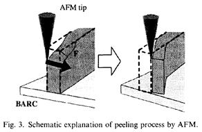 |
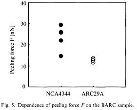 |
|
| 2006- 2. | Akira Kawai, Hotaka Endo, Tomotaka Ariga “Condensation mechanism of microbubbles depending on DFR pattern design” Microelectronic Engineering, 83, 1167-1169 (2006). |
|
| [abstract] The condensation mechanism of the microbubble is analyzed thermodynamically. Particularly, the microbubble condensation is controlled by the dry film resist (DFR) pattern design. As the bubble condensation analysis, deionized water (DI water) is dropped on a DFR pattern array. The microbubble condensed at the different position in various shape patterns. The experimental results obtained are analyzed based on the free energy balance model thermodynamically. The factor of microbubble removal from the DFR pattern is discussed for the suitable micro pattern fabrication. Keywords : Microbubble; Condensation; Etching failure; Plating failure; Micro channel |
||
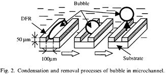 |
||
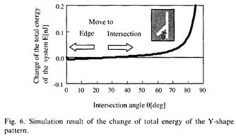 |
||
| 2006- 3. | Akira Kawai, Kenta Suzuki “Removal mechanism of nano-bubble with AFM for immersion lithography” Microelectronic Engineering, 83, 655-658 (2006). |
|
| [abstract] We discuss adhesion and removal mechanisms of nano-bubble adhered on a resist surface for immersion lithography. We employed the AFM (atomic force microscope) for the observation of nano-bubbles on a resist surface. In addition, by the thermodynamic analysis, it can be considered that the nano-bubble adhered on the resist surface tends to be a fiat shape and spread on the resist surface. It is difficult to adhere the bubbles on the resist surface. We also observed the nano-bubble adhered on both ArF and F2 excimer resist surfaces with the AFM. Keywords : Nano-scale bubble; Atomic force microscope; Immersion lithography; ArF and F2 excimer resists; Thermodynamics; Adhesion; Removal |
||
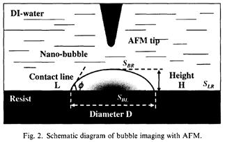 |
||
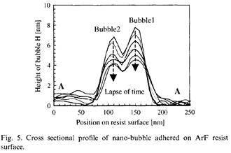 |
||
| 2006- 4. | Takayoshi Niiyama, Akira Kawai “Micro wetting system by controlling pinning and capillary forces” Microelectronic Engineering, 83, 1280-1283 (2006). |
|
| [abstract] In the recent years, wetting micro systems acting in liquid environment have been recognized as one important technology in chemical, bio and relative fields. In this regard, the micro wetting behaviors become major factors in controlling the liquid flow artificially in the micro tube, which are mainly affected by the pinning effect, capillary force, Laplace force, convection and so on. The purpose of our study is to realize the drastic control method of the wetting processes based on pinning effect and capillary forces. In this study, in order to analyze the wetting behavior precisely, we observed the spontaneous wetting processes depending on the micro pattern arrangement. From the results, the wetting phenomena can be clearly observed due to the pinning effect and capillary force. Moreover, we also found that the deionized water (DI-water) is more likely to spread on a hydrophilic surface compared with that on a hydrophobic surface. Therefore, we discuss the wetting behavior in this investigation on thermodynamics. We can control the wetting behavior practically by designing the surface energy of the resist patterns and its arrangements. Keywords : Micro wetting; Pinning effect; Capillary force; Wetting property; Resist |
||
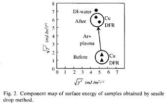 |
||
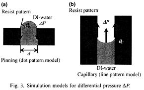 |
||
| 2006- 5. | 安江孝夫、河合 晃 「走査型プローブ顕微鏡によるシリコン酸化膜の経時絶縁破壊特性」 日本表面科学会誌、27 (4) 49-54 (2006). |
|
| [abstract] |
||
| 2006- 6. | Mitsuru Sato and Akira Kawai “Topcoat characterization for immersion lithography by fluoric acid etching on silicon substrate” J. Photopolymer Sci. Technol., 19(5), 601-611 (2006). |
|
| [abstract] For the topcoats for immersion lithography, the suppression of substance penetration is one of the most important functionalities. In order to characterize the penetration behavior, fluoric acid (HF) etching on silicon substrate is performed through a topcoat. The model topcoat is formulated with a fluorinated polymer and 2-metyl-isopropanol. The surface energy changes of silicon substrate represent the time dependency on the penetration through the topcoat. By the concentration and temperature change of the HF aqueous, it is confirmed that the penetration occurs under diffusion, and that the activation energy through the film can be neglect in comparison to that of etching the oxide layer. It is specially suggested that the diffusion should happen in the meniscus of the topcoat by the atomic force microscope observation. The diffusion coefficient for 0.5wt% HF aqueous under 20℃ is found to be 1 x 1 0-17m2/s in the 30nm film application. Keywords : topcoat, fluoric acid, surface energy, silicon, diffusion coefficien |
||
 |
 |
|
| 2006- 7. | Takayoshi Niiyama and Akira Kawai “Formation factors of watermark for immersion lithography” Jpn. J. Appl. Phys. 45, 5383-5387 (2006). |
|
| [abstract] In immersion lithography, some defects such as watermarks and nanoscale bubbles have been focused on as serious problems to be solved. To clarify the formation mechanism of the watermarks, the in-situ observations of the drying behaviors of water drops containing with particles and without particles, are conducted on Si substrates. In static watermark formation on a flat substrate, we can classify the watermark formation processes on the basis of the watermark shapes. From a surface energy balance analysis, particles dispersed in deionized (DI) water adhere on a Si substrate. In addition, owing to the Laplace force balance, the particles adhered on the Si substrate will attract surrounding particles. Hence, we can confirm the formation mechanism of the static watermark condensed in a ring shape. On the other hand, in dynamic watermark formation, we can observe clearly that a condensed watermark is formed on a Si substrate and particles move to a lower region in an inclined drop. In an actual immersion lithography system, the particles are more likely to remain in the immersion liquid under the lens system. KEYWORDS: watermark, particle, microwetting, evaporation, surface energy, pinning effect, immersion lithography, static watermark, dynamic watermark |
||
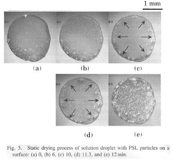 |
||
| 2006- 8. | Akira Kawai and Kenta Suzuki “Effect of low surface tension liquid on pattern collapse analyzed by observing dynamical meniscus observation” Jpn. J. Appl. Phys., 45, 5429-5434 (2006). |
|
| [abstract] It has been recognized that the decrease in surface tension of rinse water prevents resist pattern collapse during the pattern development process, We have already reported that the resist pattern collapse occurs as induced by stress concentration at the resist pattern bottom due to an air tunnel that is formed between parallel patterns. To clarify the effect of low-surface-tension liquid visibly, a transparent organic film is used as a monitoring pattern in this study, that is, direct observation through the transparent film (DOT) method. Two types of liquid: namely, (i) low-surface-tension liquid (ethyl alcohol YL = 22.5 mJ/m2) and (ii) high-surface-tension liquid [deionized (DI) water YL = 72,9 mJ/m2], are used. As a consequence, the air tunnel is not formed using the low surface tension liquid but is formed using DJ water. The balance between Laplace and elastic forces of the pattern is estimated to determine pattern collapse and deformation. As a consequence, it is effective to employ low-surface-tension liquid as rinse liquid to prevent air tunnel formation. KEYWORDS : low surface tension, Laplace force, air tunnel, pattern collapse, surface energy, meniscus, resist pattern, rinse liquid, DOT method |
||
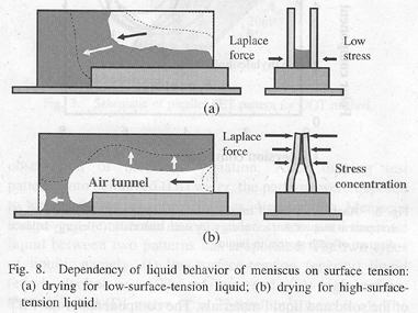 |
||
2005年 5報
| 2005- 1. | Atsushi Ishikawa, Akira Kawai “Condensation of Nano-Size Polymer Aggregates by Spin Drying” J. Adhesion and Interface, vol.6 (1) 7-10 (2005). |
|
| [abstract] Condensation control of nano-particles has become important in order to fabricate minute condensed structures. In this study, we focus our attention on condensation mechanism of polymer aggregates in a resist film. The polymer aggregate is structural component of a resist material which is used in lithography process. The condensation nature of polymer aggregates in the resist ti 1m surface is observed by using atomic force microscope (AFM). By using the AFM, the condensation of polymer aggregates can be observed clearly. The condensation of polymer aggregate strongly affects to precise fabrication of resist pattern below 100nm size. The interaction force among polymer aggregates can be analyzed based on Derjaguin approximation. We also discuss about condensation nature of polymer aggregates in the resist film surface with the help of micro sphere model. Keywords : AFM, polymer aggregate, nano-particles |
||
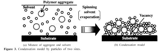 |
||
| 2005- 2. | Akira Kawai “Condensation behavior of nanoscale bubbles on ArF excimer resist surface analyzed by atomic force microscope” J. Photopolymer Sci. Technol., 18(3), 349-354 (2005). |
|
| [abstract] By using atomic force microscope (AFM), a nanoscale bubble (NB) formed on a film surface of ArF excimer resist can be imaged clearly in deionized water. The diameter and height of NBs observed are approximately 40~ 100nm and 3~8nm, respectively. By approaching the AFM tip onto the NBs, the repulsive force can be detected but the attractive force on the resist surface. The interaction analysis between the AFM tip and the ArF excimer resist surface is effective in order to identify the NBs and to distinguish from solid particles. These phenomena can be discussed on the basis of Lifshitz theory. The separation procedure of the NB is accomplished with the AFM tip. The applying load at which the NB can be separated into the minute one is approximately 5nN. Therefore, the NB is more likely to adhere to the ArF excimer resist surface than the AFM tip surface. The condensation among the NBs can be realized experimentally by the scanning with the AFM tip. Consequently, the line shape NBs of 200nm~ 1μm width and 5~ 15μm length can be formed at the scanning edge of the AFM tip. The analysis of NB nature is discussed on the point of the immersion lithography. Keywords : nanoscale bubble, atomic force microscope, immersion lithography, interaction force, Lifshitz theory, Hamaker constant, buoyancy |
||
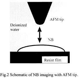 |
 |
|
| 2005- 3. | Takayoshi Niiyama, Akira Kawai “Interaction analysis of DI-water / Air / ArF resist system using atomic force microscope” J. Photopolymer Sci. Technol., 18(3), 373-380 (2005). |
|
| [abstract] In deionaized (DI) water, a removal property of nanoscale bubbles formed on an ArF excimer resist (ArF resist) film is characterized. The fundamental factors of removal property can be explained by means of interaction analysis for a Si substrate. As the interaction analyses on the Si substrate, free energy change, spreading energy, balance model between line tension and buoyancy are discussed. All analyses indicate that the removing of nanoscale bubble from the Si substrate is difficult without any additional load. In order to analyze the fundamental nature of nanoscale bubble, the nanoscale bubble is observed on the Si substrate by using atomic force microscope (AFM). The nanoscale bubble, 50nm diameter and 30nm height, can be observed on the Si substrate. Meanwhile, on the ArF resist film, the nanoscale bubble is characterized based on the above discussion. The sizes of the nanoscale bubble are 240nm diameter and 60nm height. The removal property of nanoscale bubble on the ArF resist film can be explained based on surface energy. Keywords : resist, atomic force microscope, nanoscale bubble, surface energy, immersion lithography |
||
 |
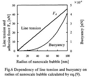 |
|
| 2005- 4. | Akira Kawai, Takahiro Moriuchi “Deflection analysis of micro cantilever due to water vapor adsorption” J. Photopolymer Sci. Technol., 18 (3), 681-682 (2005). |
|
| [abstract] Keywords : adsorption, micro cantilever, water vapor, gas sensor, QCM, sensitivity |
||
 |
 |
|
| 2005- 5. | Akira Kawai, Kenta Suzuki “Dot pattern collapse due to Laplace force analyzed by dynamical meniscus model” J. Photopolymer Sci. Technol., 18(3), 679-680 (2005). |
|
| [abstract] Keywords: Laplace force, surface energy, water meniscus, dot pattern, local wetting, pattern collapse, pattern development |
||
 |
 |
|
2004年 12報
| 2004- 1. | Akira Kawai “Influence of moving speed of AFM tip on peeling strength of micro resist pattern” J. Adhes. Soc. Technol. 40, 11-13 (2004). |
|
| [abstract] By applying a certain force directly to a resist pattern with the AFM (atomic force microscope) tip in the scanning procedure, the column shape resist pattern of 177nm diameter could be peeled easily. The peeling strength of the resist pattern increased with moving speed of the AFM tip. The influence of friction behavior between AFM tip and resist pattern on peeling strength was discussed. 原子間力顕微鏡 (AFM) の微細探針を移動させて,パターンに直接荷重を加えることにより,直径177nmサイズの円筒形レジス卜パターンを剥離した。レジス卜パターンの剥離強度は,AFM探針の走査速度の増加につれて大きくなった。パターンの剥離強度において, AFM探針とパターン間の摩擦力が及ぼす影響を考察した。 |
||
 |
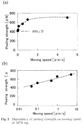 |
|
| 2004- 2. | 河合 晃、大澤義征 「角度制御型シェアモード剥離法」 Microjoining and Assembly Technology in Electronics, p77-82 (2004). |
|
| [abstract] The peeling strength of the solder bump can be determined by the angle controllable shear-mode peel (ACSP) method. By controlling the tool height and peel angle at the load position, the peeling strength for interface destruction becomes constant. By the internal stress analysis of the solder bamp, it is clarified that the stress concentration at the bump-substrate interface affects considerably to the peeling phenomena. The peeling strength of the eutectic (Sn-37Pb) and the lead-free (Sn-3.0Ag) solder bumps can be determined to be 0.11 ±0.003 and 0.31 ±0.05 GPa, respectively. Key words: Ball grid array, Interface peeling, Load angle, Shear-mode peel, Stress concentration, Finite element method |
||
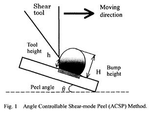 |
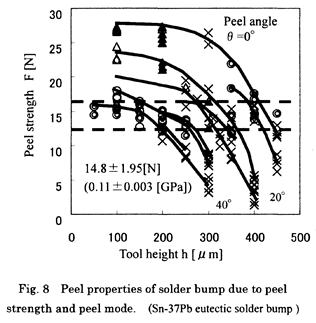 |
|
| 2004- 3. | Akira Kawai “Cohesion property of resist pattern surface analyzed by tip indentation method” J. Photopolymer Sci. Technol., 17(3), 441-448 (2004). |
|
| [abstract] By the tip indentation technique, the condensation property of resist pattern surface can be analyzed quantitatively. The fundamental property of tip indentation depending on measurement position is investigated. The pattern edge affects strongly on indenting property of a micro tip. The indenting position should be set apart from the pattern edge at least 80nm. As the representative value of surface condensation, the indentation slope value of micro tip is employed. In the indenting curve, it is clearly indicated that a certain hardened thin layer is formed on the resist surface after pattern development. These results are enhanced by the various hardening processes such as electron beam (EB) irradiation and thermal curing. One can safely state that the surface cohesion property of resist pattern can be analyzed by the tip indentation method. Keywords : surface hardened layer, tip indentation method, atomic force microscope, condensation, polymer aggregate |
||
 |
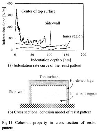 |
|
| 2004- 4. | Takayoshi Niiyama and Akira Kawai “Interaction force analysis of resist film surface in water vapor” J. Photopolymer Sci. Technol., 17(3), 453-456 (2004). |
|
| [abstract] In various humidity conditions, the interaction behavior between a resist film surface and an atomic force microscope (AFM) tip is characterized. The attractive and repulsive force due to Lenard-Jones potential can be detected clearly. In the dry condition (less than 4%RH), maximum attractive force becomes relatively small and the interactive distance becomes short. On the other hand, in the water vapor condition (70%RH), the maximum attractive force and the interactive distance become large and long, respectively. In order to analyze the interaction mechanism, Derjaguin approximation formula is employed for the AFM tip-resist system. In the attractive region, Hamaker constants in each environmental condition can be estimated. Hamaker constant in vapor condition becomes large as compared with that in dry condition. The AFM enables precise analysis for attractive interaction of resist patterns in nano-scale. It is fair certain to discuss that the micro defect such as resist fragment is attracted to the resist pattern in vapor condition. Keywords: resist, atomic force microscope, water vapor, Hamaker constant, Derjaguin approximation, attractive force |
||
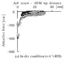 |
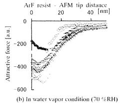 |
|
| 2004- 5. | Atsushi Ishikawa, Makoto Sakata and Akira Kawai “Meniscus analysis in micro gap during liquid drying process” J. Photopolymer Sci. Technol., 17(3), 457-460 (2004). |
|
| [abstract] The drying process of the rinse water affects strongly to pattern collapse phenomena during development process. In order to analyze the water meniscus behavior, a PET film is used as a parallel line pattern. By using this transparent pattern, wetting behavior of water meniscus between two patterns can be observed. In the drying process of water meniscus, it is clearly observed that the meniscus enters from the side edge of the parallel pattern. The meniscus behavior can be analyzed based on capillary rise and gravity. Keywords : resist pattern, rinse water, Laplace force, meniscus, pattern collapse, adhesion, gravity |
||
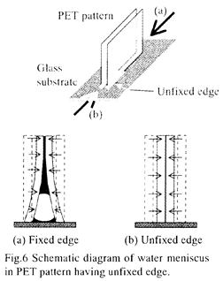 |
||
| 2004- 6. | Akira Kawai, Masahito Hirano and Takayoshi Niiyama “Analysis for drying behavior of rinse water depended on resist pattern arrangement” J. Photopolymer Sci. Technol., 17(3), 461-464 (2004). |
|
| [abstract] In the resist pattern development process, the drying behavior of the rinse water affects strongly to pattern fabrication properties such as pattern collapse, bubble capture, micro defect adhesion and so on. In order to analyze the drying speed depending on pattern arrangement, line/space and dot array patterns are fabricated. By the precipitation experiment of a solute substance, the drying behavior of the rinse water is clarified. The rinse water is more likely to remain at the dot array patterns as compared with the line/space patterns. Particularly, pinning effect which causes liquid trap around resist pattern is employed in order to explain the drying behavior. The drying model of the rinse water depended on the pattern arrangement can be constructed. Keywords : micro wetting, pinning effect, water meniscus, drying, precipitation |
||
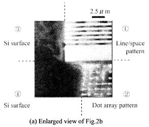 |
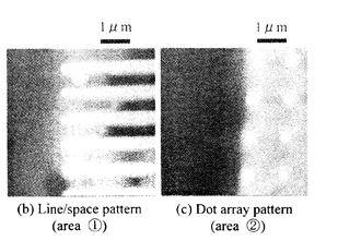 |
|
| 2004- 7. | Atsushi Ishikawa, Takashi Tanji and Akira Kawai “Cohesion property of polymer aggregate depending on hardening treatment” J. Photopolymer Sci. Technol., 17(1), 99-102 (2004). |
|
| [abstract] Condensation behavior of polymer aggregate in side-wall of resist pattern is characterized by using atomic force microscope (AFM). Various hardening process, thermal heating and EB irradiation, are performed on the resist pattern after the pattern development. The condensation of polymer aggregates in the side-wall is clearly imaged. By the hardening treatments, condensation of polymer aggregate is accelerated. The interaction force among polymer aggregates can be analyzed based on Derjaguin approximation. The condensation structure of polymer aggregate accompanying with aggregate vacancy is also discussed. Keywords : hardening, polymer aggregate, atomic force microscope, condensation,aggregate vacancy, Derjaguin approximation |
||
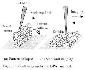 |
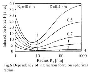 |
|
| 2004- 8. | Akira Kawai, Akihiko Seki and Hotaka Endo “Viscous finger pattern formed in photoresist film during heat treatment” J. Photopolymer Sci. Technol., 17(1), 103-104 (2004). |
|
| [abstract] Keywords : viscous finger pattern, photoresist film, Saffman-Taylor model, solvent evaporation, surface energy |
||
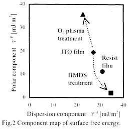 |
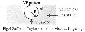 |
|
| 2004- 9. | Hotaka Endo and Akira Kawai “Micro bubbles captured at micro defect on resist film” J. Photopolymer Sci. Technol., 17(1), 105-106 (2004). |
|
| [abstract] Keywords: micro bubble, micro defect, adhesion, surface energy, pinning effect buoyancy |
||
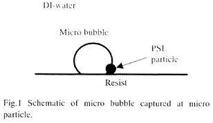 |
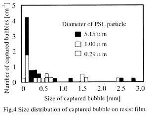 |
|
| 2004-10. | Masaki Yamanaka, Akira Okada and Akira Kawai “Pinning effect of microliquid drop on geometrical complex substrates composed with different surface energy materials” J. Vac. Sci. & Technol. B22(6), Nov/Dec 3525-3527 (2004). |
|
| [abstract] Wetting behavior of microliquid drop on a geometrical complex substrate is analyzed quantitatively. In order to analyze pinning effect in liquid spreading, the array of isolated square patterns is formed by the photolithography. The square patterns on flat substrate are composed with the combination of higher and lower surface energy materials. Two types of complex substrates, isolated polar and continuous polar patterns, are fabricated. The test liquids, de-ionized water, ethylene glycol and diiodomethane, are sessile dropped on the complex substrate. Particularly, the isolated polar pattern acts to pin the polar liquid spreading. The combination of a polar liquid and an isolated polar substrate has strong interaction on each other. However, in the case of the continuous polar pattern, the wetting behavior of liquid drop can be explained due to Cassie's equation. The contribution of the polar material to the wetting property on geometrical complex substrate can be clarified. |
||
 |
||
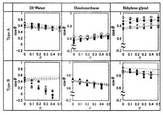 |
||
| 2004-11. | Atsushi Ishikawa, Takashi Tanji, Akira Kawai “Determination of Young's modulus of polymer aggregate based on Hertz theory” J. Photopolymer Sci. Technol., 17(5), 715-718 (2004). |
|
| [abstract] Elastic property of polymer aggregates in a resist pattern is characterized by using atomic force microscope (AFM). In order to determine Young's modulus of polymer aggregates based on Hertz theory, a separation force between polymer aggregates is measured by using the AFM. Young's modulus of polymer aggregates composing resist pattern can be determined to be lO-25MPa. The results of our experiment clearly show that the polymer aggregates indicates relatively low cohesion property. Keywords : resist, polymer aggregate, Young's modulus, atomic force microscope, Hertz theory, separation force |
||
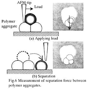 |
||
| 2004-12. | Hotaka Endo, Akira Kawai “Adhesion mechanism of micro bubbles on ArF and F2 excimer resists” J. Photopolymer Sci. Technol., 17(5), 713-714 (2004). |
|
| [abstract] Keywords : micro bubble, ArF excimer resist, F2 excimer resist, adhesion, surface energy, pattern defect |
||
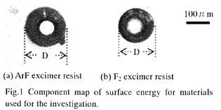 |
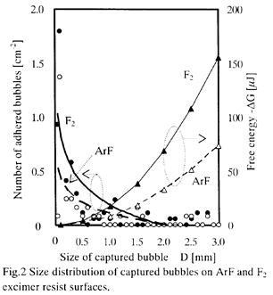 |
|
2003年 10報
| 2003- 1. | Akira Kawai, Daisuke Inoue “Effect of Thermal Stress on Peel Property of Line Resist Pattern Analyzed by Atomic Force Microscope (AFM)” J. Adhes. Soc. Technol. 39, 107-109 (2003). |
|
| [abstract] The improvement of adhesion property of micro resist pattern has been recognized as one important problem in nano-device fabrication. By the heat treatment, the thermal stress concentrates at a vicinity of line edge of resist pattern. By the direct peeling method with atomic force microscope (AFM), it is clarified that the pattern peel is more likely to occur at the pattern edge. By combining with stress analysis, the close relationship between thermal stress concentration and peeling property is confirmed. |
||
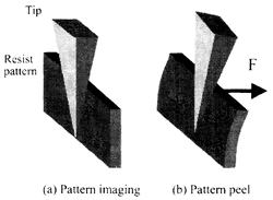 |
 |
|
| Fig.2 Pattern peel by the DPAT method | Fig.3 SEM photograph of line resist pattern | |
| 2003- 2. | Daisuke Inoue, Akira Kawai “Peeling Analysis of Resist line Pattern of 170nm Width Due To Crack Formation by using Atomic Force Microscope Tip” Surface and Coating Technology, 169-170, pp.311-315 (2003). |
|
| [abstract] A quantitative analysis of the dependency of the line pattern peeling on the load position is carried out by using an atomic force microscopy tip. The load for pattern peeling F decreases as approaching the load position to the pattern edge, therefore, the pattern edge of the line pattern is more likely to peel. The internal stress and its distribution of the line resist pattern due to crack generation is simulated by the three-dimensional finite element method (3D-FEM) as comparing with the experimental results. By the crack generation. the load F, simulated for pattern peeling by the 3D-FEM decreases as the comparison with no crack model. The simulated results of the load position dependency is similar to the experimental results. In combination with the stress analysis, the peeling mechanism of micro structure accompanying with crack generation can be clarified. Keywords : Atomic force microscopy; Nanostructure: Interfaces: Elastic properties |
||
 |
 |
|
| Fig.1 Schematic explanation of the DPAT method with the AFM tip. | Fig.2 Dependency applying load F for pattern peel on the load position d. Five pieces of the line pattern were tested at each load position. |
|
| 2003- 3. | Akira Kawai, Daisuke Inoue “Van der Waals interaction between Si surface and micro tip apex treated with hexamethyldisilazane (HMDS)” J. Adhes. Soc. Technol. 39, 255-258 (2003). |
|
| [abstract] Dependency of attractive force on interaction distance between tip apex and solid surface can be measured directly by using atomic force microscope (AFM). By treating the tip apex with hydrophobic agent (hexamethyldisilazane, HMDS), the maximum force and its interaction length become low and short, which are due to van der Waals (vdW) and hydrogen bond interactions. The result has a correlation to the analysis data of surface energy. It seems reasonable to suppose that the adhesion and dispersion properties of micro condensed matters can be analyzed by using AFM. 原子間力顕微鏡 (AFM) の微細探針を用いて,探針と基板間の相互作用力(引力)の距離依存性を直接測定できる。探針先端にHMDS (hexamethyldisilazane)を用いた疎水化処理を行うことにより,ファンデルワールス相互作用および水素結合に起因した引力は減少し,かつ,近距離になった。以上の結果は,表面エネルギーの結果に相関があり,微小固体の吸着および分散制御に有効である。 |
||
 |
 |
|
| Fig.1 Schematic explanation of the interaction between tip apex and substrate surface. | Fig.3 The interaction curve between AFM tip and Si suhstrate. | |
| 2003- 4. | Akira Kawai “Cohesion property of resist micro pattern analyzed by using atomic force microscope (AFM)” J. Photopolymer Sci. Technol., 16(3), 381-386 (2003). |
|
| [abstract] Condensation properties of polymer aggregate are characterized by the typical AFM techniques, collapse, separation, indentation and manipulation. The association of polymer aggregate of approximately 50nm size is clearly observed in the resist surface. By the separation technique, the cohesive property of associated polymer aggregate is analyzed. It is clearly indicated that two associated polymer aggregates are separated into 13 pieces of aggregates. The interaction force among polymer aggregates can be analyzed based on Derjaguin approximation. By the tip indentation, the condensation of polymer aggregate accompanying a certain vacancy can be analyzed. The polymer aggregate of 20nm size can be manipulated and rearranged in linear position. One can safely state that polymer aggregate is regarded as a granular solid material which has a certain cohesive strength. The condensation model of polymer aggregate accompanying with vacancy resist is introduced. Keywords: resist, polymer aggregate, atomic force microscope, separation, indentation, manipulation, Derjaguin approximation |
||
 |
 |
|
 |
||
| 2003- 5. | Naotaka Kubota, Tomohiko Hayashi, Takeshi Iwai, Hiroshi Komano, Akira Kawai “Advanced resist design using AFM analysis for ArF lithography” J. Photopolymer Sci. Technol., 16(3), 467-474 (2003). |
|
| [abstract] We found that the line edge roughness (LER) of resist pattern could be improved by improving the uniformity of the polymer itself, the main component of the photoresist, at stage of the polymerization. Also, we found that, by using the atomic force microscope (AFM), the aspect of the polymer aggregates had difference when we quantitatively comparison-measured photoresist surface, which was in process of dissolution. We believe that this difference is due to the individual aggregate dissolution property toward the developer. In this paper, we are focusing on the dissolution property of polymers toward developer, and discussing on the uniformity of the polymer and the correlation to the LER. Keywords: ArF, resist, lithography, line edge roughness (LER), surface roughness, polymer aggregate, atomic force microscope (AFM) |
||
 |
||
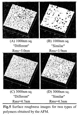 |
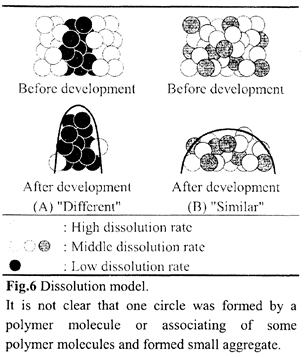 |
|
| 2003- 6. | Akira Kawai “Adhesion of ArF Excimer Resist Pattern Depending on Heating Temperature Analyzed by Atomic Force Microscope” J. Adhes. Soc. Technol. 39, 423-425 (2003). |
|
| [abstract] By using the atomic force microscope (AFM), the adhesion property of the micro organic pattern of 177nm diameter, which is fabricated by ArF excimer laser lithography, can be analyzed quantitatively. In the ranging of heating temperature from 100 to 200°C, the peeling strength of resist pattern increases with the increase of heating temperature. Particularly, the adhesion property is improved clearly above 150°C. This technique will give useful information for adhesion designing of micro structure system. 原子問力顕微鏡(AFM)の微細探針を用いることで,基板上に付着している微細有機パターンの付着性を定量解析することができる。ArFエキシマレーザーを用いて作製した直径177nmの円筒形レジス卜パターンに対し,100~200°Cの範囲で熱処理を行った。その結果,熱処理温度の増加と共に,レジストパターンの剥離強度も増加することを確認した。特に, 1500°C以上において付着性が大きく改善した。この手法は,微細構造体の接着設計において有効な手段となる。 |
||
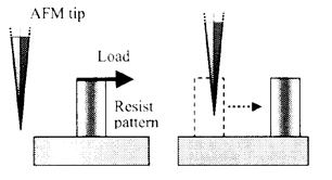 |
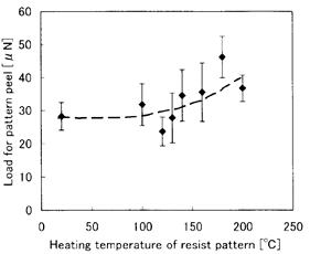 |
|
| (a)Applying load (b)Pattern peel Fig.1 Schematic explanation of the peeling procedure with an AFM tip. |
Fig.3 Dependency of the load for pattern peel on heating temperature. | |
| 2003- 7. | Akira Kawai, Yuji Sawanaga “Condensation control of micro particles by charge deposition method” J. Photopolymer Sci. Technol., 16(5), 669-670 (2003). |
|
| [abstract] Keywords : micromachining, particle, condensation, scratching, AFM |
||
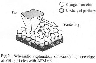 |
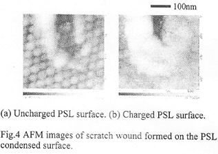 |
|
| 2003- 8. | Akira Kawai, Junko Kawakami “Characterization of SiO2 surface treated by HMDS vapor and O2 plasma with AFM tip” J. Photopolymer Sci. Technol., 16(5), 665-668 (2003). |
|
| [abstract] In order to prepare hydrophobic and hydrophilic surfaces, silane coupling treatment with hexamethyldisilazane (HMOS) and exposing to oxygen plasma are carried out to silicon oxide substrates, respectively. Surface force measurement indicates that the attractive force F of the AFM tip is more sensitive to surface energy variation of the solid surface. The adhesion work W mainly depends on polar component of surface energy. Positive correlation between elastic energy Ee of the cantilever tip and adhesion work W can be confirmed. By using two kinds of tips which have different component values of surface energy, surface property in lithography process can be analyzed. Keywords : adhesion, AFM, HMDS, surface energy, micro machine |
||
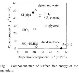 |
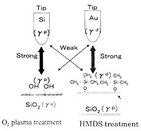 |
|
| Fig.6 Interaction model between the tip and the sample surfaces. | ||
| 2003- 9. | Masahito Hirano, Akira Kawai “Adhesion of AFM tip to resist surface due to Laplace force” J. Photopolymer Sci. Technol., 16(5), 663-664 (2003). |
|
| [abstract] Keywords : resist, adhesion, meniscus, Laplace force, atomic force microscope |
||
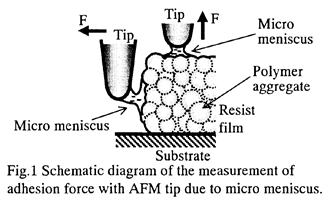 |
 |
|
| 2003-10. | Takayoshi Niiyama, Yuji Sawanaga, Akira Kawai “Determination of electrified area formed by AFM lithography” J. Photopolymer Sci. Technol., 16(5), 661-662 (2003). |
|
| [abstract] Keywords : AFM lithography, attractive force, contact electrification, resolution |
||
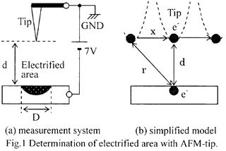 |
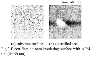 |
|
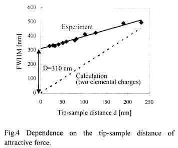 |
||
2002年 9報
| 2002- 1. | Akira Kawai, Takato Abe “Analysis of Pattern Collapse of Electron Beam Resist Ranging from 60 to 152 nm Width with Atomic Force Microscope Tip” J. Adhesion Soc. Japan, 38 16-19 (2002). |
|
| [abstract] Quantitative analysis of collapse property of an electron beam (EB) resist pattern ranging from 60 to 152 nm width and 220 nm height is demonstrated experimentally. By directly applying a load to a top corner of resist pattern with micro-cantilever tip, resist line pattern adhering on a subsutrate can be collapsed easily accompanying slight residue formation. The load required for collapsing pattern decreases linearly with decreasing the pattern width of resist pattern. The pattern collapse occurs in the cause of insufficient cohesion of the resist material. |
||
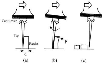 |
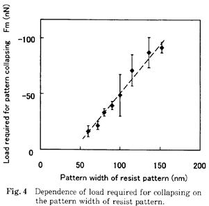 |
|
| Fig.2 Schematic explanation of collapse process. Tip movement was controlled vector scan program and monitored simultaneously. | ||
| 2002- 2. | 河合 晃 「探針の吸着力測定による水蒸気の凝縮性解析」 日本接着学会誌、38, 50-53 (2002). |
|
| [abstract] へき開したマイ力表面を基板として、探針の吸着力の相対湿度依存性を測定した。相対湿度を4%RHから70%RHの範囲で変化させた場合、探針の吸着力はS字型の吸着曲線を示すとともに、ヒステリシス特性を有することが分かった。探針の吸着力変化は、基板上での首位上記の凝縮過程を反映している。これらを、探針と基板間のメニスカス形成の観点から考察した。 Humidity dependency of adsorption force of microtip on cleaved mica surface is analyzed. In the range of 4 to 70%RH, a S-type curve and hysteresis properties of tip adsorption are observed. The adsorption property reflects the moisture condensation process on the substrate. The tip substrate adsorption property can be analyzed due to meniscus formation. |
||
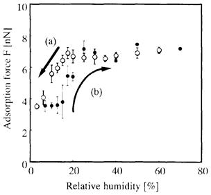 |
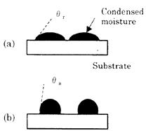 |
|
| Fig.2 ependency of micro tip adsorption on relative humidity. |
Fig.4 Schematic explanation of contact angle change of condensed nucleus.
(a): drying process, (b): humidifying procpss. |
|
| 2002- 3. | 河合 晃 「水蒸気吸着に伴う微細カンチレバーの撓み変位の解析」 日本接着学会誌、38, 169-172 (2002). |
|
| [abstract] 両面を異なる材質で構成した微細カンチレバーを大気中に暴露した場合,湿度変化に応じて微細カンチレバーにたわみ変位が生じる。Au膜とSi3N4膜を微細カンチレバーの上下面に形成した場合,相対湿度の増加に伴ってレバーはSi3N4膜側へたわんだ。また,カンチレバーの両面をAu膜で形成した場合は,たわみ変位は殆ど生じなかった。すなわち,微細カンチレバーのたわみ変位は,レバーの上下面への水蒸気の吸着特性に対して差動的に'生じると考えられる。これらのメカニズムを,固体表面での水蒸気のクラスター核生成における活性化エネルギーの点から考察した。微細カンチレバーのたわみ変位を利用することにより,湿度センサーとしての応用が期待できる。 By exposing a micro cantilever which is composed by different two materials to vapor atmosphere, slight deflection of micro cantilever due to humidity change can be observed. As increasing relative humidity, the micro cantilever composed by Au and Si3N4 multilayer films bends slightly toward the side of Si3N4 thin film. When the both sides of micro cantilever is composed by the same material, no deflection can be detected. The micro cantilever has a differential sensitivity to moisture adsorption onto each surface of the micro cantilever. Based on activation energy at nucleation of moisture cluster, deflection mechanism of the micro cantilever can be analyzed. It is capable to apply the micro cantilever as a humidity sensor. |
||
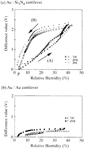 |
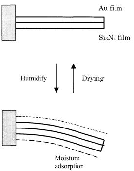 |
|
| Fig.2 Relationship between relative humidity and deflective displacement of micro cantilever due to moisture adsorption. |
Fig.4 Differential deflection model of micro cantilever due to moisture adsorption |
|
| 2002- 4. | Akira Kawai “Adhesion and Cohesion Properties of Dot Resist Patterns Ranging from 84 to 364 nm Diameter Analyzed by Direct Peeling Method with Atomic Force Microscope Tip” J. Photopolymer Science & Technology, 15(1), 121-126 (2002). |
|
| [abstract] By directly applying a load to top comer of a resist pattern with a microcantilever tip,a dot resist pattern adhering on a flat substrate can be collapsed easily by accompanied with slight residue. By the synchrotron radiation (SR) lithography, the dot resist patterns ranging from 84 to 364 nm diameter and 550 nm height are formed on the Si(100) substrate. The static load applied by the cantilever, which is required for pattern collapse, decreases with decreasing the pattern diameter and is proportional to the cross-sectional area of the resist pattern. In combination with the stress distribution analysis, the mechanism of pattern collapse and residue formation can be clarified. The pattern collapse occurs by the stress concentration at the pattern bottom slightly away from the interface. It is clear that the pattern collapse can be dominated by the stress concentration in the resist pattern. Keywords : resist, adhesion, collapse, atomic force microscope, lithography, fracture,internal stress, finite element method |
||
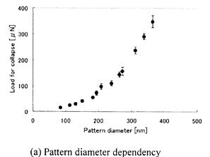 |
 |
|
| Fig.6 Collapse property for these different diameter patterns. | ||
| 2002- 5. | Akira Kawai, Daisuke Inoue “Van der Waals Interaction between Polymer Aggregates and Substrate Surface Analyzed by Atomic Force Microscope (AFM)” J. Photopolymer Science & Technology, 15(1), 127-132 (2002). |
|
| [abstract] The peeling property of the resist pattern can be analyzed on the point of van der Waals (vdW) interaction between polymer aggregates and substrate by using the atomic force microscope (AFM). By treating the substrate with hexamethyldisilazane (HMDS), the interaction length between tip and substrate is shorten and weakened. It is clarified that a part of polymer aggregates condensed at pattern bottom have no contribution to the interaction with the substrate because the interaction length becomes short. At the resist-substrate interface, a certain vacancy among the polymer aggregates is found out. Based on the aggregation model, it is clarified that exposing the substrate to HMOS vapor acts to weaken the peeling strength of the resist pattern. Keywords: polymer aggregate, adhesion, peeling, atomic force microscope, surface energy, vacancy, silane-coupling treatment |
||
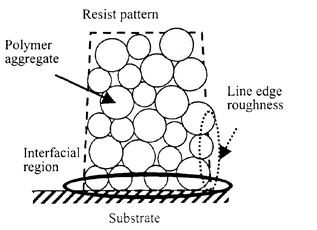 |
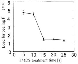 |
|
| Fig.5 Schematic of resist pattern condensed by polymer aggregates. |
Fig.8 Experimental result with regard to pattern peel property by DPAT method. | |
| 2002- 6. | Akira Kawai “Cohesion Property of Polymer Aggregates in Resist Pattern Analyzed by Atomic Force Microscope (AFM)” J. Photopolymer Science & Technology, 15(3), 371-376 (2002). |
|
| [abstract] By using a micro cantilever tip of atomic force microscope (AFM), polymer aggregates condensed in a line resist pattern can be manipulated. A vacancy of polymer aggregate is found out at the resist-substrate interface, which acts to induce the subsequent etching failure and to weaken cohesion strength of the resist pattern. Quantitative analysis of collapse property of an electron beam (EB) resist pattern ranging from 60 to 152 nm width and 220 nm height is demonstrated experimentally by using the AFM tip. The load required for pattern collapse decreases with decreasing the pattern width. Internal stress and deformation analysis based on the aggregate model explains well the collapse property of the line resist pattern. Keywords: atomic force microscope, polymer aggregates, manipulation, vacancy,pattern collapse, adhesion |
||
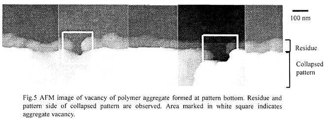 |
||
| 2002- 7. | Akira Kawai, Daisuke Inoue “Peeling Property of Resist Pattern in Water Analyzed by Atomic Force Microscope” J. Photopolymer Science & Technology, 15(5), 757-758 (2002). |
|
| [abstract] Keywords: adhesion, peeling, atomic force microscope, surface free energy, liquid environment, intrusion |
||
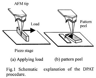 |
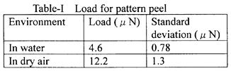 |
|
| 2002- 8. | Akira Kawai “Resist Pattern Peel due to Resonance Effect of Micro Tip” J. Photopolymer Science & Technology, 15(5), 759-760 (2002). |
|
| [abstract] Keywords: resist, adhesion, peel, resonance, atomic force microscope, lithography, stress |
||
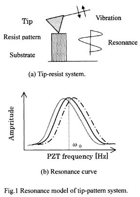 |
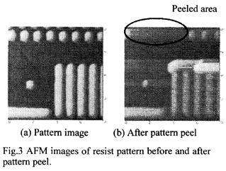 |
|
| 2002- 9. | Hideaki Yoshida, Tadashi Nakamura, Yoshiaki Kawakami, Akira Kawai “Establishment of Eaves Forming Model by Analysis of the Interface Energies at the Threefold of Cu/DFR/Ni Plating Solution” J. Adhesion Soc. Japan, 38, 413-419 (2002). |
|
| [abstract] Eaves formation is a problem that occurs in a micro-plating pattern in DFR (Dry Film photoResist) lithography. From SEM (Scanning Electron Microscope) observation and XMA (X-ray MicroAnalysis) identification, it is found that a cross-sectional shape of eaves is like bird's-beak. As a factor of eaves formation, it is found that the adhesion energies balance at the threefold of Cu substrate /DFR/developer solution. Thus, a developer is likely to intrude into the interface of Cu substrate/DFR to form a micro gap. However, the bird's-beak like eaves is not merely caused by the gap (however it is formed). It was found that the Ni plating solution intrudes into the Cu substrate/DFR interface, and the shape of eaves is formed with the growth of the plating. From these results, we propose a model of the eaves formation. |
||
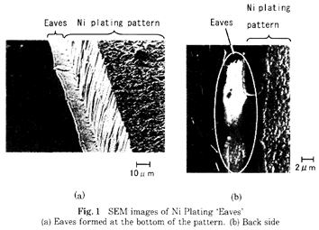 |
||
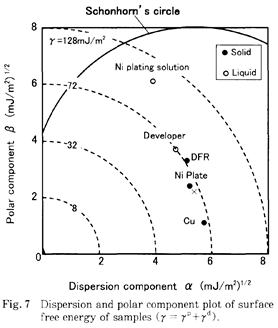 |
||
2001年 12報
| 2001- 1. | 河合 晃、堀口博司 「原子間力顕微鏡を用いた微細探針と無機固体表面間のHamaker定数解析」 日本接着学会誌、37, 146-149 (2001). |
|
| [abstract] 物質間に働くファンデルワールス相互作用を表す物理量の一つにHamaker定数がある。Hamaker定数A[J]は, 固体表面において, 曲率半径R[m]の微細探針の吸着力F[N]を測定することにより実験的に求められる。また, Lifshitz理論によれば, Hamaker定数Aは, 探針材料および試料表面の屈折率nと比誘電率εを用いて理論的に求めることができる。本研究は, これらの異なる手法で求めたHamaker定数間に正の相関があることを確認し, 微細探針を用いた物質間のHamaker定数解析の有効性を示した。また, 材料の異なる探針を用いることにより, 測定試料の材質同定技術の可能性を議論する。 Hamaker constant between two solid surfaces is one important physical factor due to van der Wasl’s interaction. By measuring the adsorption force F[N] to the solid surface with a micro tip (curvature radius of tip apex R[m]), Hamaker constant A[J] can be obtained experimentally. Meanwhile, based on Lifshits theory, Hamaker constant A between solid surfaces can be calculated with refractive index n and relative dielectric constant ε of the tip-sample materials. In this study, the positive correlation between two Hamaker constants obtained by these different methods is clearly confirmed. The validity and effectiveness of Hamaker constant analysis by the probe method can be confirmed. The possibility of indentification of sample materials by this method is also discussed. |
||
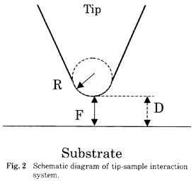 |
||
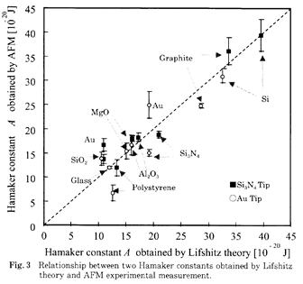 |
||
| 2001- 2. | Akira Kawai, Norio Moriike “Analysis of Pattern Collapse of ArF Excimer Laser Resist by Direct Peeling Method with Atomic Force Microscope Tip” Microelectronic Engineering, vol.57-58, pp683-692 (2001). |
|
| [abstract] Quantitative analysis of the collapse property of dot resist pattern formed by ArF excimer laser lithography ranging from 141 to 405 nm diameter and 360 nm height is demonstrated experimentally. By directly applying a load to a top corner of the resist pattern with a microcantilever tip, a resist dot pattern adhering on a substrate can be collapsed easily accornpanying slight residue formation. The load required for pattern collapse decreases with decreasing pattern diameter. In combination with an analysis of the internal stress distribution in the resist pattern, destruction mechanisms and the diameter dependency of pattern collapse can be clarified. Keywords : Resist: Adhesion: Collapse: Atomic force microscope: Lithography: Fracture: Polymer |
||
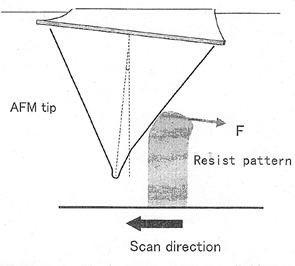 |
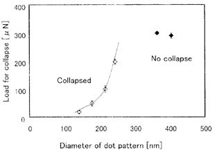 |
|
| Fig.3 Schematic explanation of DPAT process. The tip movement was controlled by a vector scan program and monitored simultaneously. |
Fig.4 Dependence of load for collapse on the diameter of dot pattern. |
|
| 2001- 3. | Akira Kawai, Norio Moriike “Adhesion and Cohesion Analysis of ArF/SOR Resist Patterns with Microtip of Atomic Force Microscope (AFM)” J. Photopolymer Science and Technology, 14(4), 507-512 (2001). |
|
| [abstract] By directly applying load to a top corner of dot resist pattern with a microcantilever tip, a dot pattern adhering on a substrate can be deformed and collapsed easily. The elastic and adhesion properties of a dot resist pattern can be analyzed quantitatively. The SOR (synchrotron orbital radiation) resist patterns ranging from 84 to 36 nm diameter and the ArF resist pattern ranging from 141 to 405 nm diameter are used for the investigation. In combination with an analyzed of the double spring model, Yong’s modulus of the SOR resist pattern can be determined to be 1.2 GPa. The applying load required for pattern collapse decreases with decreasing the pattern diameter, and it is proportional to the cross-sectional area of the resist pattern. This technique gives useful information to the field of structural designing of resist material. Keywords : atomic force microscope, adhesion, peeling, Young’s modulus |
||
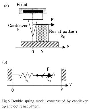 |
 |
|
| 2001- 4. | Akira Kawai, Takato Abe “Direct Measurement of Resist Pattern Adhesion on the Surface with Silane-coupling Treatment by Atomic Force Microscope (AFM)” J. Photopolymer Science and Technology, 14(4), 513-518 (2001). |
|
| [abstract] It is well known that the silane-coupling treatment with HMDS (hexamethyldisilazane) has an effect to prevent collapsing a resist pattern in a liquid environment but to decrease adhesion strength between a resist and a substrate. Dependency of resist pattern peeling on the exposing time to the HMDS vapor is investigated in a dry condition. The peeling strength of the resist pattern adhering on the substrate is determined by means of the direct peeling with atomic force microscope tip (DPAT) method. The load for pattern peeling decreases gradually as the exposing time to the HMDS vapor increases and is clearly explained by analyzing the adhesion energy. The slight change of the surface chemistry such as silane-coupling treatment can be analyzed directly by the DPAT method. Keywords : adhesion, peeling, atomic force microscope, surface energy |
||
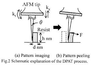 |
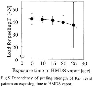 |
|
| 2001- 5. | 原 朋敬、小泉延恵、河合 晃 「Glass/レジスト/Cu/Al/Glass多層構造の破壊特性解析」 日本接着学会誌、37, 303-308 (2001). |
|
| [abstract] 多層構造内のレジスト膜を熱処理すると、レジスト膜中に含まれる溶剤の蒸発によって粘性指状 (VF: Viscous Fingering) の微小空隙が多数形成される。本研究では、空隙形成に伴うレジスト膜の応力緩和と応力集中に注目して、Glass/レジスト/Cu/Al/Glass多層構造の破壊特性解析を行った。実験では、レジスト膜によって張り合わされたGlass基板とCu/Al/Glass多層基板間の破壊強度を、引張り試験機を用いて測定した。その結果、レジスト膜中の空隙面積の増加に伴いレジスト膜の破壊強度が高くなることと、空隙周辺ではAl/Glass界面での剥離が生じることを見出した。有限要素法による応力分布解析により、これらの現象の原因が、空隙形成に伴うレジスト膜の内部応力緩和と、空隙周辺部での応力集中であることを見出した。 When the resist adhesive layer inserted in the Glass / resist / Cu / Al / Glass multilayer structure is heated, the micro void due to VF (Viscous Fingering) phenomenon is formed in the resist adhesive layer during the solvent evaporation. The purpose of this paper is to analyze the destruction property of the Glass / resist / Cu / Al / Glass multilayer structure with regard to the stress concentration and stress relaxation of the resist adhesive layer due to void formation. The destruction strength of the resist adhesive layer inserted in the multilayer structure was measured by using the peeling tester. As the result, the destruction strength of the multilayer structure increases with increasing the number of void in the adhesive layer. Moreover, the Al / Glass interface destruction occurs extensively around the each void. It is considered that the destruction phenomena were due to stress relaxation of resist adhesive layer and to stress concentration around the void, respectively. |
||
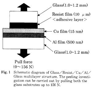 |
||
|
||
| 2001- 6. | 阿部貴人、河合 晃 “原子間力顕微鏡(AFM)を用いた線幅60nmのラインレジストパターンの弾性解析” 日本接着学会誌、37, 353-357 (2001). |
|
| [abstract] 近年、ミクロな視点から、固体の付着・凝集特性を解析する技術の開発が望まれている。本論文では、原子間力顕微鏡 (AFM:Atomic force microscope) の微細探針を用いて、微細レジストパターンに直接荷重を加える手法により、その弾性特性を解析する。実験では、線幅が60nmの電子線用化学増幅型レジストパターンのバネ定数の導出を試みる。まず、先端形状の異なる3種類の微細探針を用いて、実験条件の最適化を行った。次に、微細探針とレジストパターンから構成される連結バネモデルを考えることで、レジストパターンのねじれのバネ定数を算出した。その結果、バネ定数を403N/mと見積もることができた。本論文では、AFMを用いたレジストパターンの弾性解析の妥当性を考察する。 Recently, on the microscopic point of view, quantitative analysis method of adhesion and cohesion properties for micro-condensed matter is strongly desired. In this paper, by using an atomic force microscope (AFM) tip, elastic property of micro resist pattern is analyzed by applying a certain load with a cantilever tip directly. A chemically amplified resist pattern of 60 nm width, which is sensitive to the electron beam irradiation, is used for the investigation. A spring constant of the line resist pattern is estimated based on the double spring model. Three kinds of cantilever tip, which have different shape of tip apex, are evaluated in order to obtain a clear image of the nanoscale pattern. Consequently, the spring constant of the line resist pattern is determined to 403 N/m. The validity of this method by using AFM is discussed. |
||
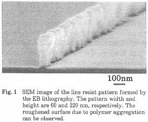 |
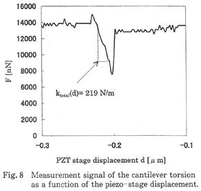 |
|
| 2001- 7. | Akira Kawai, Norio Moriike “Resist Hardening by Electron Beam Irradiation Analyzed by Atomic Force Microscope” J. Photopolymer Science and Technology, 14(5), 751-752 (2001). |
|
| [abstract] Keywords : atomic force microscope, hardening, electron, beam, refractive, index |
||
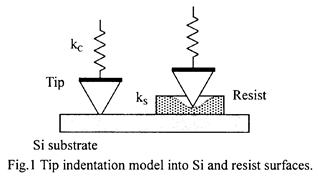 |
 |
|
| 2001- 8. | Akira Kawai “Collapse of Dot Patterns Formed on Various Substrates analyzed by Tip Scanning Method” J. Photopolymer Science and Technology, 14(5), 723-724 (2001). |
|
| [abstract] Keywords : adhesion, atomic force microscope surface energy, pattern collapse |
||
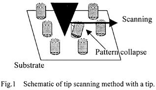 |
 |
|
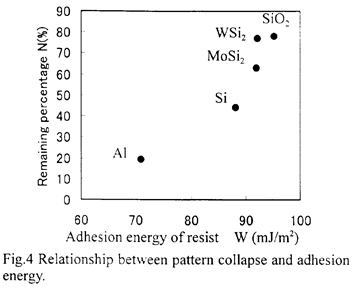 |
||
| 2001- 9. | Akira Kawai, Yoshihisa Kaneko “Estimation of Young’s Modulus of Resist Pattern by using Atomic Force Microscope” J. Photopolymer Science and Technology, 14(5), 731-734 (2001). |
|
| [abstract] By applying a certain load directly with a micro cantilever tip, an elastic deformation of resist micro pattern adhering on a substrate can be characterized quantitatively. By combining with finite element analysis of resist pattern deformation, Yong’s modulus of micro resist pattern of 190 nm width and 770 nm height formed by KrF excimer laser lithography can be obtained. Young’s modulus of resist pattern is estimated in the range of 4to 5 GPa, which is similar to those of typical polymer materials. Keywords : KrF excimer resist, Young’s modulus, atomic force microscope, adhesion, elastic deformation |
||
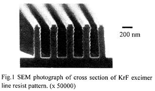 |
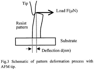 |
|
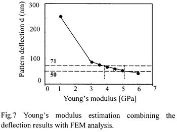 |
||
| 2001-10. | Akira Kawai, Yoshiaki Kawakami “DUV Hardened Layer of Resist Dot Pattern Detected by Tip Indentation Method” J. Photopolymer Science and Technology, 14(5), 749-750 (2001). |
|
| [abstract] Keywords : hardening, DUV curing, atomic force microscope, indentation, collapse |
||
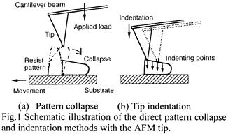 |
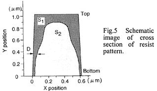 |
|
| 2001-11. | Akira Kawai, Yoshihisa Kaneko “Fatigue Property of Resist Micro Pattern Analyzed by Atomic Force Microscope Tip” J. Photopolymer Science and Technology, 14(5), 701-702 (2001). |
|
| [abstract] Keywords :fatigue, adhesion, collapse, atomic force microscopy, resist, internal stress |
||
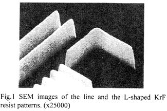 |
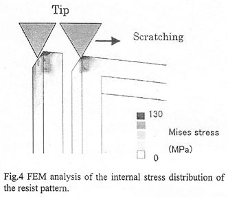 |
|
| 2001-12. | 磯部 亮、河合 晃 「微細周期パターン上へのプラズマ重合膜の堆積特性」 日本接着学会誌、37, 433-436 (2001). |
|
| [abstract] フォトレジスト材料で形成された周期パターン上へHMDSO (hexamethyldisiloxane) 重合膜をプラズマCVD法により堆積した。パターン周期は、0.39~1.5μmの範囲で変化させた。断面形状の観察から、重合膜の堆積特性を評価した。平坦性の指数として、周期パターンの凹部と凸部における、基板から重合膜表面までの高さの比を用いた。パターン周期が約0.75μmにおいて、平坦性の閾値があることが分かった。閾値以上のパターン周期では、平坦性指数は約0.5となった。また、閾値以下では良好な平坦性となったが、重合膜中にボイドが形成された。重合膜中のボイドの形成メカニズムを考察した。 By means of plasma CVD (Chemical vapor deposition), a HMDSO(hexamethyldisiloxane)polymeric film is formed on a periodic pattern consisting of photoresist. Pattern pitch is ranging from 0.39 to 1.5μm. The deposition property is evaluated by SEM (scanning electron microcopy) observation. As the flatness factor, height ratio of polymeric film surface at concave and convex positions of the periodic pattern. At the pattern pitch of 0.75μm, the threshold of flatness is observed. Above the threshold, flatness factor is approximately 0.5. Below the threshold, good flatness is confirmed, however, micro void is formed. Mechanism of void formation is discussed. |
||
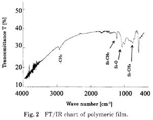 |
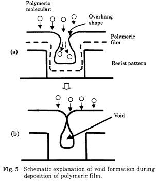 |
|
2000年 8報
| 2000- 1. | Akira Kawai “Collapse Behavior of Organic Dot-Pattern Analyzed by the Tip Indentation Method” J. Adhesion Soc. Japan, 36, 23-27 (2000). |
|
| [abstract] By applying a certain load directly with a microcantilever tip, a resist micropattern adhering to a substrate can be collapsed accompanying a residue formation. By combining with the finite element method for the internal stress anal., it is clear that the crack formed in the resist micropattern affects the stress distribution and the residue shape. By the tip indentation method, the collapse and destruction mechanism of the resist micropattern can be analyzed. |
||
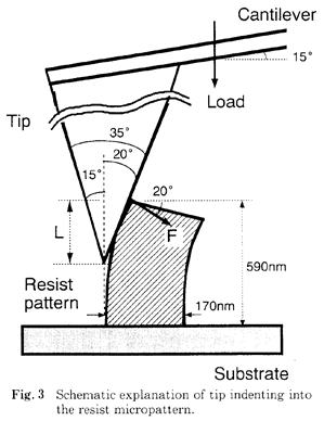 |
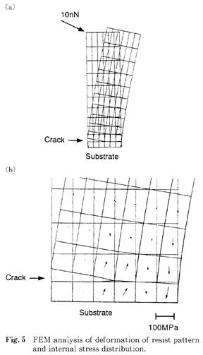 |
|
| 2000- 2. | 河合 晃、川上喜章 “原子間力顕微鏡(AFM)を用いた微細探針走査法によるフォトレジスト微細パターンの接着性解析” 日本接着学会誌、36, 2-9 (2000). |
|
| [abstract] 原子間力顕微鏡 (AFM : Atomic force microscope) を用いて,サブミクロンサイズのフォトレ ジストパターンの接着および凝集性解析を試み,この手法の妥当性を議論する。フォトレジストパターンとして, 平坦基板上の高さ1.01μm,幅060μmのドット形状のものを一個選択し,微細探針から直接荷重を掛けながら走査することで倒壊させる。そして,倒壊に要した荷重,および倒壊直前のパターン歪みを測定する。このパターン歪み測定と有限要素法による応力変形解析との組み合わせにより,界面剥離を引き起こす要因となった内部応力およびパターンのヤング率を算出する。 これらの値は,フォトレジストパターンの熱処理温度の増加に伴って大きくなることが分かった。この傾向は、フォトレジスト膜の熱重量(TG)と硬度および屈折率などの熱処理温度依存性と密接な相関を示しており,本手法の妥当性を確認した。本手法は,フォトレジストパターンなどの微細構造体の接着および凝集特性を直接解析する上で有効である。 By using an atomic force microscope (AFM) , we discuss validity of analysis method of adhesion and cohesion property of micro photoresist pattern. Dot shaped photoresist patterns, 0.6μm in square and 1.01μm in height were formed onto a flat substrate by photolithography. Load for collapse of photoresist pattern and its deflection are measured by applying load with an AFM micro tip. By combining with stress and deformation analysis by finite element method, internal stress for collapse and Young’s modulus of the photoresist pattern can be obtained. These value increase with heating temperature of photoresist pattern. By the thermal analysis of weight loss, hardness and refractive index, we confirmed the validity of this method. This method can be applied to adhesion and cohesion analysis of micro condensed matter adhered on a flat substrate. |
||
 |
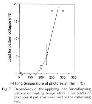 |
|
| 2000- 3. | Akira Kawai, Yoshihisa Kaneko “Analysis of Resist Pattern Collapse by Direct Peeling Method with Atomic Force Microscope Tip” Jpn. J. Appl. Phys., 39, 1426-1429 (2000). |
|
| [abstract] Quantitative analysis of the adhesion property of a KrF resist pattern is demonstrated experimentally. Dependency of the load for collapse on various line and L-shaped patterns, is investigated. By directly applying normal load with a microcantilever tip, a photoresist pattern adhering on a substrate can be collapsed easily. The adhesion strength of the L-shaped pattern is considerably large as compared with the line pattern. The reliability of this method is discussed together with the analysis of stress distribution in the KrF resist patterns. KEYWORDS : adhesion, collapse, atomic force microscopy, resist, finite-element method, internal stress, residue |
||
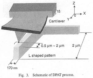 |
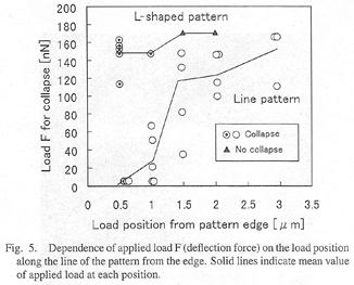 |
|
| 2000- 4. | 河合 晃 “固体表面での微細探針の吸着力解析” 日本接着学会誌、36, 131-135 (2000). |
|
| [abstract] 原子間力顕微鏡 (AFM) を用いることにより、固体表面間の相互作用力の直接測定が可能となる。しかし、原子レベルで平坦な基板はマイカやグラファイトのへき開などでしか得られず、殆どの固体表面は表面粗さ (Rms) に代表されるような微小な凹凸を有している。また、通常の大気中では水蒸気が固体表面に吸着しており、AFMの探針と基板間にメニスカスが形成されてラプラス力が働くようになる。一般に、球/平面間の吸着式としては、F = 4pRrで表されるDerjaguin近似が代表的である。本報では、薄膜の表面粗さ (Rms) を0.25~12.8nmの範囲、γを40~69mJ/m2、相対湿度を4%と40%に変化させて、微細探針の吸着力に及ぼす各要因の影響を考察した。その結果、これらの範囲においては、薄膜の表面粗さが吸着力測定に最も影響することが分かった。AFMを用いて固体表面の吸着力測定を精度高く行うためには、固体の表面粗さを少なくとも3nm程度に抑えること、あるいは表面粗さ効果を補正することが重要となる。 The direct measurement of interaction force between 2 condensed matters is capable by using atomic force microscopy (AFM). An atomic flat surface can be obtained by cleavage of mica or graphite. Most of solid surfaces indicate micro roughness represented as square mean roughness Rms. Moreover, in ordinal ambient condition, a certain moisture adsorbed on any solid surfaces and a meniscus between micro tip and sample surface is formed. Generally, adsorption force between a microsphere and a flat surface can be represented as F = 4pRr, Durjaguin approximation. Influence of surface roughness (Rms:0.25~12.8 nm), surface energy (40~69 mJ/m2) and relative humidity (4% and 40%) on micro-tip adsorption is studied. Consequently, it is clarified that surface roughness of the sample has strongly affected to the adsorption force. For the precise measurement of adsorption force, surface roughness at least less than 3nm is required. |
||
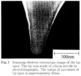 |
 |
|
| 2000- 5. | 河合 晃 “マイカへき開表面での微細探針の摩耗に伴う吸着力変化” 日本接着学会誌、36, 172-175 (2000). |
|
| [abstract] マイカを劈開することによって原子スケールで平坦な表面を形成し、その表面における曲率半径20nmの微細探針 (Si3N4製) の摩耗特性を解析した。探針先端の摩耗によって生じるマイカ表面での接触面積変化に注目し、探針の吸着力変化として摩耗特性を解析した。マイカ表面での探針の摩耗は、探針に荷重0.5nNを掛けながら、走査速度が16.3μm/sで12.8mmの距離を滑らせることで行った。それにより、約0.3μmの深さの摩耗が生じた。マイカ表面での探針の吸着力は、滑り距離が長くなるにつれて増加することを見出した。よって、摩耗による探針先端の僅かな形状変化を吸着力変化として検出できることを示した。 The wear property of the microtip apex (curvature radius of apex: 20nm) made of Si3N4 can be analyzed by sliding on the cleavaged mica surface. Separation force of the tip apex from the mica surface increases with the sliding distance on the mica surface. Increment of the adsorption force is affected by the increase of contacting area of the tip apex to the mica surface. One can safely state that the slight deformation of microtip apex by wearing can be detected and analyzed by measuring the adsorption force of microtip |
||
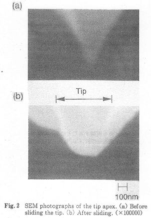 |
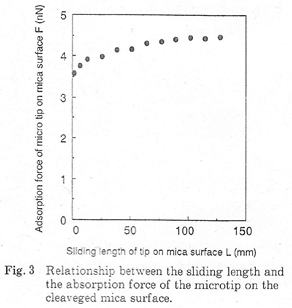 |
|
| 2000- 6. | 森池教夫、河合 晃 “原子間力顕微鏡を用いた一括破壊試験法による有機ドットパターンの付着挙動解析” 日本接着学会誌、36, 295-301 (2000). |
|
| [abstract] 半導体素子製造のプロセスに用いられる有機ドットパターンに原子間力顕微鏡 (AFM) の探針から荷重を加えて破壊することで、パターンの付着力を直接に解析できる。今回、KrFエキシマレーザー対応科学増幅型レジスト (直径110~240nm) のパターン破壊荷重の度数分布の簡便な測定法を新たに提案し、その破壊挙動を解析する。ドットパターンの破壊荷重依存性には閾値が存在する。よって、閾値荷重及び初期不良パターン数からレジストパターンの付着信頼性を評価できる。AFMによるその場観察から、パターン破壊後の基板表面にはレジスト残渣が観察された。よって、パターン自身が凝集破壊していることがわかった。また、本手法をArFエキシマレーザー対応科学増幅型レジストにも適用して妥当性を確認した。そして、3次元の有限要素法により、加重時に発生するパターン内部の応力分布を解析した。これにより、応力集中がパターン破壊に大きく影響していることを明らかにした。 A resist dot-pattern adhering on substrate can be removed precisely by applying a certain load with an atomic force microscope tip. The applying load for the pattern destruction is reflected strongly by the adhesion force of the resist pattern. In this paper, we propose a quantitative and statistical method for analyzing the destruction property. Concretely, the destruction property of KrF excimer laser chemically amplified resist is analyzed by this method. The reliability of this method is evaluated with the threshold load and the number of initial failure patterns. The pattern collapsed easily when the cohesion strength of resist material is relatively low, because certain pattern residue can be observed on the substrate. Then, the desutruction force for ArF excimer laser chemically amplified resist was also analyzed by this method. A stress distributed in a resist pattern is also calculated by three-dimensional finite element method. The residue formation of dot- patterns is strongly affected by the stress concentration at a vicinity of interface. |
||
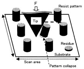 |
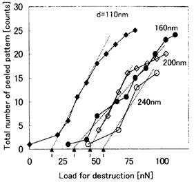 |
|
| Fig.4 Schematic diagram of the concept of novel method for pattern destruction with the AFM tip. |
Fig.7 Dependency of load for destruction on diameterof KrF excimer resist patterns. |
|
| 2000- 7. | 森池教夫、河合 晃 “原子間力顕微鏡を用いた微細レジストドットパターンの疲労解析” 日本接着学会誌、36, 404-407 (2000). |
|
| [abstract] 原子間力顕微鏡 (AFM) の探針から微細レジストパターンに荷重を加えて破壊することで,パターンの破壊荷重を定量測定できる。直径が160nmであり, 高さが593nmであるドット形状パターンに, 一定荷重を繰り返し加えることで疲労破壊を引き起こした。疲労がない場合のパターンの破壊荷重は約90nNであった。しかしながら, 疲労を加えた場合は, 1.3nNや53.lnNの低荷重でもパターン破壊が生じた。荷重を105nNまで増加させた場合, 顕著に破壊が生じた。本手法により, パターン内部に蓄積される疲労を評価できることを確認した。 The destruction load of the micro resist pattern is measured quantitatively by means of applying load with an atomic force microscope (AFM) tip. By the fatigue effect, the dot-shaped pattern of 160nm in diameter, to which the constant load is applied repeatedly with the AFM tip, is destructed. The destruction load without fatigue effect is approximately 90nN. However, with fatigue effect, the pattern destruction occurs even at lower load, 1.3 and 53.1nN. The results indicate the pronounced fatigue effect by increasing the applying load until 105nN. This method can be useful for the quantitative analysis of fatigue effect in micro scale. |
||
 |
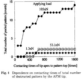 |
|
| 2000- 8. | Akira Kawai “Collapse Behavior of KrF Resist Line Pattern Analyzed with Atomic Force Microscope Tip” Jpn. J. Appl. Phys., 39, 7044-7048 (2000). |
|
| [abstract] A quantitative analysis of the adhesion property of a KrF line resist pattern of 170nm width is carried out experimentally. By directly applying load to the top corner of the resist pattern with a microcantilever tip, a resist line pattern adhering on a substrate can be collapsed easily and is accompanied by residue formation. The dependency of line pattern collapse on load position along with line direction is investigated. At the load position 3μm away from the pattern edge, the average load required for the pattern collapse is about 15 times larger than that of the load position at the pattern edge. Based on this result, one can confidently state that the pattern edge is more likely to collapse. In combination with the analysis of the internal stress distribution of the resist pattern, the load position dependency of the pattern collapse and the destruction mechanisms of the resist-substrate interface can be clarified. It is also clear that the crack formed at the pattern bottom affects the stress concentration and the residue shape. KEYWORDS : adhesion, collapse, atomic force microscopy, resist, finite-element method, internal stress, residue, destruction, cohesion, crack, lithography, KrF excimer laser |
||
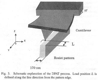 |
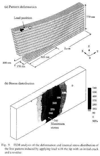 |
|
1999年 2報
| 1999- 1. | Akira Kawai “Collapse Behavior of Micro Resist Pattern Analyzed by Tip Indentation Method with Atomic Force Microscope” J. Vac. Sci. & Technol. B17, 1090-1093 (1999). |
|
| [abstract] A novel method for quantitative analysis of the adhesion property of a resist micropattern is demonstrated exptl. By applying a normal load directly with a microcantilever tip, a photoresist micropattern adhering to a substrate can be collapsed easily. The load, when the pattern collapse occurred, increased with the heating temperature of the resist pattern. The detectable sensitivity of this method can be estimated as less than 0.1 nN. The validity and reliability of this method are discussed by comparing with the adhesion result of the conventional peeling test. |
||
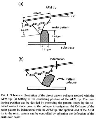 |
 |
|
| 1999- 2. | 河合 晃 「Cu/Al多層膜構造の破壊強度に及ぼすAl自然酸化膜の影響」 日本接着学会誌、35, 558-561 (1999). |
|
| [abstract] 高集積半導体デバイス(LSI)などの金属配線に多用されるCu/Al多層膜構造において、微細加に伴う強度改善が重要な課題となっている。特に、大気暴露したAI膜表面には自然酸化膜が容易に形成されるが、剥離試験の結果、この自然酸化膜層において破壊が生じていることが分かった。また、自然酸化膜層の存在により、Cu膜とAI膜とのミキシング膜の形成が妨げられていることが分かった。このように、界面に存在する自然酸化膜は、多層膜構造の接着強度に大きく影響を及ぼすことが分かった。 The improvement of destructive strength of Cu ? Al multilayer structure is regarded as one of the important problems on the view point of micro electronic device fabrication. However, native oxide layer can be formed easily on aluminum film surface by exposuring to air. By the destruction test of the multilayer structure, it is found that the interface destruction occurs mainly at the native oxide layer on the aluminum film. Moreover, the native oxide of Al film prevents to form intermixing layer between Cu and Al layers. The native oxide layer strongly affects to adhesion strength of multilayer. |
||
 |
 |
|
| Fig.1 Change of wetting property of deionized water on aluminum surface on lapse of time after exposure to air. Contact angle was measured at 30 sec after sessile drop on the aluminum film. | Fig.4 Elemental line analysis of Al and Cu by means of EPMA. The analyzed area is the destructed sample in Fig.3(a). | |
1998年 5報
| 1998- 1. | 河合 晃 「10nm以下のAu薄膜の成長挙動と接触角変化」 日本接着学会誌、34, 209-213 (1998). |
|
| [abstract] 平均膜厚0.2~10nmのAu薄膜に対して、グリセリンの接触角の膜厚依存性を解析した。グリセリンの接触角は,約2.0nm以上の膜厚で急増し飽和することを見いだした。また、この膜厚は,Au薄膜の抵抗率がバルク (2.2×10⁻⁸Ωm) 領域になる膜厚にも相当する。これらの結果を,Maxwell Garnett理論に基づくAu微粒子の分極率サイズ効果とAu薄膜表面のモフォロジーの点から解析する。 Thickness dependency of contact angle on gold thin film is studied. Contact angle of grycerol increases rapidly and saturates over 2.0nm in thickness. Moreover, the resistivity of gold film corresponds to the bulk value (2.2×10⁸-8Ωm) at this thickness. These results are analyzed on the points of size effect of polarizability for gold micro particle based on Maxwell Garnett theory and surface morphology of gold thin film. |
||
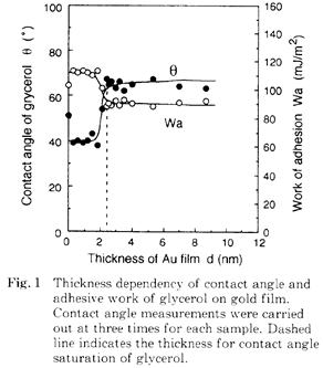 |
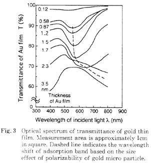 |
|
| 1998- 2. | 河合 晃 「ミクロンサイズの格子型基板を用いた液滴平面形状の制御」 日本接着学会誌、34, 226-228 (1998). |
|
| [abstract] 基板上に作製したミクロンサイズの正方形格子パターンの高さと周期を変えることにより、基板上の平面形状は八角形や正方形に変形する、また、平坦基盤に対する表面積比rが約1.5以上になると、この液滴歪みが顕著になる。これは、各格子パターンが液滴の拡がりに対する抑制のポテンシャルとして働き、かつ、拡がり方向によって単位長さ当たりの格子パターン数が異なるためと考えられる。 Lattice structure in microscale fabricated on a substrate has an effect to change the planer shape of liquid drop. By changing the height and width of the periodic lattice pattern, drop shape can be modified into octagon or square in high sensitivity. If surface area ratio r of real substrate to ideal one becomes over 1.5, the modification of drop shape occurs drastically. Each lattice pattern acts as the preventive potential for liquid spreading. By the anisotropy of number of lattice pattern in spreading direction, these deformation of liq. drop can be explained. |
||
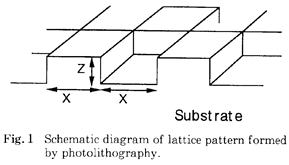 |
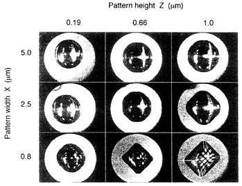 |
|
| Fig.2 Photographs of liquid drop shape in planer view observed by using optical microscope. | ||
| 1998- 3. | Akira Kawai “Characterization of Fall Angle of Water Drop based on Surface Energy Components” J. Adhesion. Soc. Japan, 34, 191-193 (1998). |
|
| [abstract] Experimental results of fall angle based on thermodynamics are shown. Surface energies of each substrate and liquid are obtained by the contact angle method. Fall angle decreases as surface energy of substrate increases. These phenomena have close dependency of polar interaction based on van der Waal’s force between liquid and solid interface. |
||
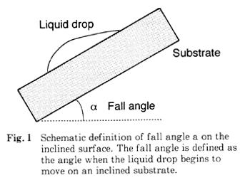 |
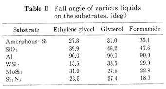 |
|
| 1998- 4. | 河合 晃、岡田 彰 「異種材料で構成された格子状基板上での液滴の接触角」 日本接着学会誌、34, 22-25 (1998). |
|
| [abstract] 表面エネルギーの異なる2種類の材料を用いて格子状基板を作製し, 液体のぬれ挙動を解析した。各材料の面積割合とパターン配置を変えて純水の接触角を測定し, Cassieの式に基づき結果を解析した。接触角の低い材料が局在するパターン配置の場合, 液滴の拡がりは制限される。その結果, 液滴形状は歪み, Cassieの式には従わないことが明らかになった。 The wetting property of liquid on a lattice substrate, which is composed of two sets of materials, is analyzed. The contact angles of liquid on these materials are different. The fraction of materials is controlled by changing the pattern arrangement. The contact angle of deionized water on these substrates are analyzed based on Cassie’s eguation. The spreading of liquid drop is restricted at the low contact angle surface localized in the pattern arrangement. Therefore, the drop shape distortion causes deviation from Cassie’s eguation. |
||
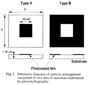 |
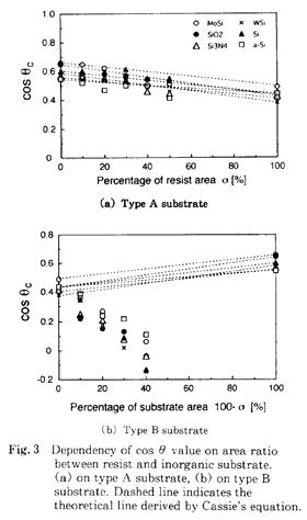 |
|
| 1998- 5. | 堀口博司、河合 晃 「AFM探針とポリスチレンラテックス(直径42nm~1μm)凝集粒子間の付着力解析 -DMT理論に基づく微粒子系の相互作用力の補正式-」 日本表面科学会誌、19, 491-497 (1998). |
|
| [abstract] 凝縮したポリスチレンラテックス(PSL)粒子とAFM探針の相互作用力のPSL粒子直径依存性を,乾燥雰囲気中で測定したフォースカーブにより調べた。PSL粒子の直径が42nm~1μmの範囲では,この直径依存性はDMT理論から求めた平均半径による依存性とは異なっていた。これらの結果をPSL粒子変形効果と隣接PSL粒子寄与により解析した。この解析において,微粒子系での力の粒径依存性の観点からDMT理論によるvan der Waals力の幾何平均半径の補正を提案した。 Dependence of interaction force between condensed polystyrene-latex (PSL) particles and atomic force microscope (AFM) tip on diameter of PSL particle is studied from the force curve measured in dry atmosphere. In the diameter range of PSL particle from 42 nm to 1μm, it is found that this dependence is different from that of geometric mean radius which is derived from DMT theory. These results can be analyzed in terms of PSL particle deformation effect and contribution of surrounding PSL particles. |
||
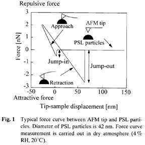 |
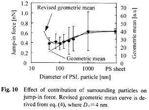 |
|
1997年 4報
| 1997- 1. | 河合 晃 「原子間力顕微鏡(AFM)によるフォトレジスト膜表面の摩擦挙動解析(周期パターンの歪検出方式)」 日本接着学会誌、33, 465-471 (1997). |
|
| [abstract] 原子間力顕微鏡 (AFM) の微細探針を用いて, 試料表面の像観察を行う場合, 像が歪む。 これは, 探針と試料表面間の摩擦に応じてカンチレバーがゆがむことに起因している。そこで, 周期的に配列されたホールパターンをフォトレジスト膜に形成し, 摩擦による観察像の周期歪を定量化した。この手法を用いて, フォトレジスト膜上でのAFM探針の摩擦挙動を解析した。その結果, フォトレジスト膜を150℃でベーク処理した場合, 摩擦力が最小となることを見い出した。この摩擦挙動を, 探針の吸着力, 表面自由エネルギー, 基板の表面粗さ, 吸着水によるラプラス力の点から解析した。この手法で, 固体表面の摩擦挙動を精度よく解析できる事を示した。 In the AFM measurement, a surface image contains a distortion based on a lateral bending of micro cantilever tip. The friction force between micro tip and substrate surface affects to this lateral bending. In this study, the friction property of photoresist surface are characterized by measuring a periodical distortion of the hole pattern. The min. friction of photoresist film was found at the baking temp. of 150℃. The temperation dependency of friction behavior has analyzed in terms of adsorption force, surface free energy, roughness and Laplace force. This method is useful to detect the surface friction property of various solid surfaces. |
||
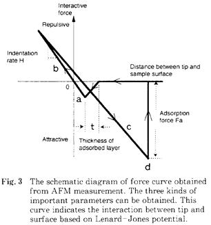 |
 |
|
| 1997- 2. | 河合 晃、芦田安立 「AFM微細探針によるAu表面の弾性および吸着特性」 日本接着学会誌、33, 395-397 (1997). |
|
| [abstract] 原子間力顕微鏡 (AFM) の微細探針 (曲率半径:40nm) をAu基板表面に接触させ,吸着力の押し込み深さ依存性を解析した。押し込み量が大きい程,探針の吸着力が増加することがわかった。これは,探針とAu表面間の接触面積の増加が原因であると考えられる。これらを,Au表面の弾性特性および有限要素法による変形解析により考察する。 By contacting a micro tip (40nm: curvature of apex) onto a gold substrate surface, the dependency of adsorption force on indentation depth is analyzed. As increase of the indentation depth of tip, the adsorption force increases. The increase of contact area between tip and gold surface would affect to the interaction between two surfaces. This result is analyzed on the point of elastic property of gold film and on deformation analysis based on finite element method. |
||
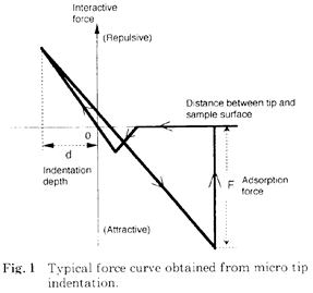 |
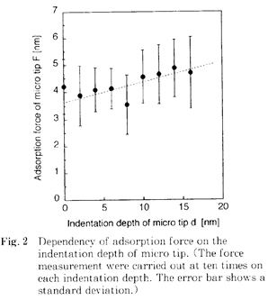 |
|
| 1997- 3. | Wataru Wakamiya, Makoto Hirayam, Akihiko Yasuoka, Akira Kawai “Refractive Index Distribution in Photoresist Thin Film Formed by the Spin Coating Method” Jpn. J. Appl. Phys., 36, L1622-L1624 (1997). |
|
| [abstract] By measuring refractive index distribution in a wafer, we discuss the characteristic change of resist film. By various treatments including baking and dipping into a solution, the refractive index distribution differs slightly from that of the resist thickness in wafer. We analyzed the refractive index variation based on the Clausiu-Mossotti relation of a solid. KEYWORDS : photoresist, intrusion, spin coat, refractive index, LSI, solvent, film thickness, permittivity, Clausius-Mossotti relation |
||
 |
 |
|
| fig.3 Distribution change of both thickness and refractive index from TMAH aqueous solution dipping. | Fig.4 Dependency of refractive index, density and residual solvent of photoresist film on baking temperature. | |
| 1997- 4. | 河合 晃、小泉延恵 「溶剤蒸発に伴うレジスト膜の粘性指状変形と接着性」 日本接着学会誌、33, 434-437 (1997). |
|
| [abstract] 2枚のスライドガラスで挟んだレジスト膜をベーク処理した場合、フラクタル的な粘性指状の変形 (VF変形) がレジスト膜内に生ずる。これは、ギャップ間で急激に溶剤がガス化したことが原因であり、レジスト膜のベーク処理を急速に行うほどVF変形は顕著になる。また、VF変形度が高くなるにつれて、レジストとガラス間の接触面積は減少し接着強度は低下する。Saffmanのモデルを用いて、レジスト膜のVF現象を解析した。 Elastic deformation of a resist film, which contains a solvent, is studied for the glass/resist/glass system. The viscous fingering (VF) pattern is formed in the resist film by the solvent evaporation. Moreover, this phenomenon is enhanced by the rapid baking of photoresist film. By the VF pattern formation, the adhesive strength between the resist film and the glass substrate decreases with effective contact area between two surfaces. The VF deformation, in this case, can be analyzed on the basis of Saffman’s model. |
||
 |
||
1996年 6報
| 1996- 1. | 河合 晃、熊谷武司、高田雅介 「遷移金属薄膜上に形成したBaTiO3薄膜の熱処理時の接着挙動」 日本接着学会誌、32, 404-409 (1996). |
|
| [abstract] 将来の高集積半導体メモリ用のキャパシタ材料として、BaTiO3薄膜は数多く研究されている。電極材料として用いられる遷移金属薄膜 (Pt, Pd, Au) と誘電体材料であるBaTiO3薄膜との接着機構を研究した。各電極薄膜上にBaTiO3薄膜をスパッタリング法で堆積し、熱処理を行った後での膜剥離を光学顕微鏡で観察した。BaTiO3薄膜はPt薄膜と最も接着性が良いが、Pd薄膜およびAu薄膜上では比較的弱い。原子間力顕微鏡による表面観察により、熱処理による電極薄膜表面の形状変化とBaTiO3薄膜との接着力に相関があることを見い出した。また、接触角法により求めた各薄膜の表面自由エネルギーの解析により、電極薄膜とBaTiO3薄膜間の接着仕事と接着力にも相関があることを見い出した。 |
||
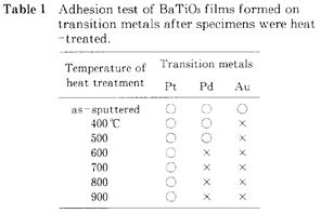 |
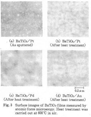 |
|
| 1996- 2. | Akira Kawai “Measuring the Thermal Properties of Photoresist Thin Films Using Atomic Force Microscopy” Thin Solid Films, 273, 308-311 (1996). |
|
| [abstract] Dependency of the surface hardness on the baking temperature of the resist film is studied. By using a micro-tip mounted in an atomic force microscope, the surface hardened layer of the resist film can be detected. On the other hand, knoop hardness measurement has no sensitivity to the surface hardness. The adsorption force of the atomic force microscope micro-tip has no correlation to the surface free energy of the resist film. The hardness behavior is affected by the solvent evaporation from the resist film. These results can be explained by the indentation model which contains the elastic deformation of the resist surface. Keywords : Atomic force microscope: Hardness: Evaporation |
||
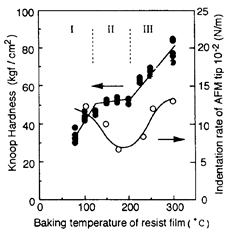 |
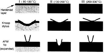 |
|
| Fig.1 Dependency of knoop hardness and indentation rate of the AFM tip on the baking temperature of a resist film. | Fig.7 Indentation model between tip and resist surface. |
|
| 1996- 3. | 河合 晃 「スパッタリングで形成したAuおよびPtの大気中放置に基づく表面自由エネルギー変化」 日本接着学会誌、32, 39-43 (1996). |
|
| [abstract] 真空中で形成したAuおよびPt薄膜を大気中に放置したときの表面自由エネルギーの経時変化を、接触角測定および原子間力顕微鏡 (AFM) での吸着力測定により解析した。時間の経過とともに、Au薄膜の分散成分γdは増加し、極性成分γpは減少し、これらの和である表面自由エネルギーγは減少する。これらの値は約30分後に一定になる。一方、Pt薄膜の場合は、大気中へ出した直後から分散成分γd, 極性成分γpとも殆ど変化しない。これらの挙動は、各薄膜表面の分散相互作用の大きさの違いにより説明できる。Au薄膜表面ではPt薄膜より分散相互作用が大きいため、有機物の吸着が優先的に生じると考えられる。原子間力顕微鏡により実測した表面吸着力の経時変化は、表面自由エネルギー変化と一致する結果であった。 Surface free energy variation of sputtering-formed Au and Pt thin films after exposure to air is studied by measuring the contact angle and adsorption force using atomic force microscopy. With the time after exposure to air, the dispersion component γd of Au film increases, while polar component γp decreases. Surface free energy γ, the sum of γd and γp, also decreases. These values leveled off about 30 min after exposure to air. On the other hand, the values of γd, γp, and γof Pt film are almost constant. These phenomena can be explained in terms of the difference in dispersion interaction between the two film surfaces. The organic adsorption occurs preferentially on the Au surface, since it has a large dispersion interaction. The time dependence of adsorption force measured by atomic force microscopy is similar to that of surface free energy. |
||
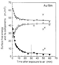 |
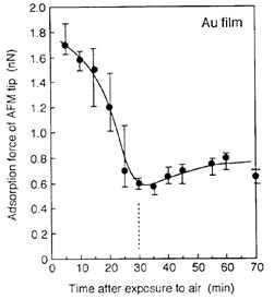 |
|
| Fig.2 Variation of surface free energy and its dispersive and polar components of Au film surface after exposure to air. Measurement error of contact angle is less than 4%. |
Fig.5 Variation of adsorption force of AFM tip on Au surface.Measurements are carried out five times at the different position. Both average and range among measurement data are indicated. |
|
| 1996- 4. | Akira Kawai, Takeshi Kumagai and Masasuke Takata “Correlation between Surface Free Energy and Dielectric Constant of BaTiO3 Thin Film” J. Adhesion Society of Japan, 32, 221-223 (1996). |
|
| [abstract] By measuring surface free energy γ of BaTiO3 thin films, its dielectric behavior can be characterized. The Polar (Keesom) component γP of surface free energy is directly proportional to dielectric constant (εr) on the other hand, dispersion (London) component γd has no correlation. These mechanism are discussed in terms of behavior of dipole moment in the BaTiO3 film. |
||
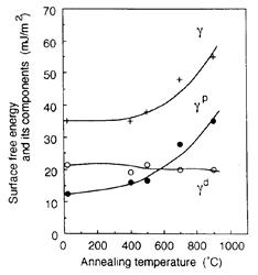 |
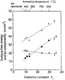 |
|
| Fig.1 Dependency of surface free energy on annealing temperature of BaTiO3 thin film. Measurement error of contact angle is less than 4%. | Fig.2 Relationship between dielectric constant and surface free energy of BaTiO3 thin film. | |
| 1996- 5. | Wataru Wakamiya, Makoto Hirayama, Akihiko Yasuoka and Akira Kawai “Adhesion Improvement of Photoresist on TiN/Al Multilayer by Ozone Treatment” Jpn. J. Appl. Phys., 35, L1227~L1229 (1996). |
|
| [abstract] The effect of ozone treatment on photoresist adhesion is studied in terms of thermodynamics. The peeling strength of a photoresist-substrate joint is iscreased by a factor of about two by ozone treatment. An increase in the surface free energy of the substrate is responsible for this adhesion improvement. KEYWORDS : adhesion, photoresist, ozone, surface free energy, wetting, contact angle, corona discharge, strength, atomic force microscope, antireflectivecoating, aluminum, titanium nitride |
||
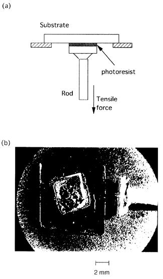 |
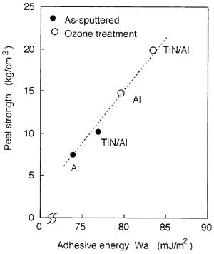 |
|
| Fig.1 Test system for resist/substrate adhesion strength. (a) Schematic diagram of a test sample. (b) Photograph of a sample after the peel test. A rod 2.5mm in diameter was adhered to the sample and then peeled. | Fig.2 Correlation between peel srrength and adhesive work Wa. | |
| 1996- 6. | 若宮 亙、平山 誠、安岡晶彦、河合 晃 「フォトレジスト膜へのアルカリ水溶液の浸透と接着性」 日本接着学会誌、32, 294-297 (1996). |
|
| [abstract] フォトレジスト膜中へのアルカリ水溶液の浸透により基板との接着力は低下する。アルカリ水溶液としてテトラメチルアンモニウムヒドロキシド (TMAH) の2.38%の水溶液を用い,フォトレジスト膜の屈折率の低下及び膜厚の増加によりTMAH水溶液の浸透を確認した。フォトレジスト膜へのTMAH水溶液の浸透が平衡に達した後,レジストマイクロパターンは基板から加速的に剥離することを見い出した。 The intrusion of alkaline aqueous solution into photoresist film is responsible for decrease of adhesion strength to the substrate. TMAH (tetramethylamrnoniumhydroxide) aqueous solution of 2.38% conc. is used as the alkaline aqueous solution. Decrease of refractive index and increase of film thickness indicate the intrusion of TMAH aqueous solution. After equilibrium of intrusion is reached, it is found that the adhesion failure of resist pat tern is accelerated. |
||
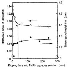 |
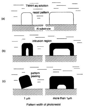 |
|
| Fig.3 Dependency of refractive index and thickness of photoresist film on dipping time into TMAH aqueous solution. |
Fig.4 Schematic diagrams of intrusion of THAM aqueous solution and peeling of resist pattern. (a)immediately after dipping into TMAH aqueous solution. (b)intrusion of TMAH aqueous solution into photoresist film. (C)equilibrium of intrusion is almost reached. | |
1995年 11報
| 1995- 1. | 永田一志、河合 晃 「Al薄膜の表面粗さとレジスト微細パターンの接着性」 日本接着学会誌、31, 44-48 (1995). |
|
| [abstract] 半導体集積回路 (LSI) の製造技術の中で、フォトレジスト微細パターンの接着技術は今後重要な分野となる。配線材料であるアルミニウム薄膜上のレジストパターンの接着において、アルミニウム薄膜の表面粗さの影響を研究した。三種類の平均粗さ (Ra=2.0, 5.5 11mm) のアルミニウム薄膜において、5.5mmの粗さのものが最も大きい接着力を示した。この結果は表面粗さの増加に伴う二つの要因:( i ) 基板界面付近のレジスト内の応力集中の発生、( ii ) レジストとアルミニウム表面の接触面積の増加で説明できる。 In Large Scale Integrated Circuit (LSI) production, the adhesion control of a photoresist micro pattern to a substrate has become important. Dependency of resist adhesion on surface roughness Ra=5.5 nm among three kinds of surface roughness. This result can be explained by two factors: (i) stress concentration at the interface region. (ii) increase of the contact area between resist and substrate surface, as the surface roughness increases. |
||
 |
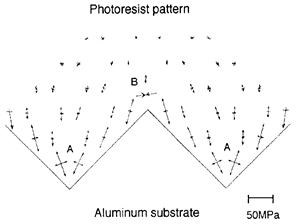 |
|
| Fig.4 Histdyagrams of adheslon test with 70 test chips. |
Fig.5 Finite element analysis of stress concentration atthe resist / substrate interface. | |
| 1995- 2. | 永田一志、河合 晃 「フォトレジスト膜の残留歪みと接着性に及ぼす溶剤の効果」 日本接着学会誌、31, 187-191 (1995). |
|
| [abstract] レジスト膜中の溶剤濃度を真空処理によりコントロールし、レジスト現像時の膜歪みと接着性に及ぼす影響を研究した。レジスト中の溶剤濃度が高いほどレジスト膜の残留歪みの発生は抑制されるが、現像時の接着性は低下することがわかった。また、レジスト膜の歪み変動は、膜の屈折率変化として現れることを見い出した。レジスト膜の残留歪みの抑制と接着性の向上の両方を満足させるには、溶剤濃度のコントロールが重要である。 The effect of solvent concentration in photoresist thin on residual strain and adhesion during development is studied. The solvent concentration is controlled by means of vacuum evaporation. The generation of residual strain is prevented as the solvent concentration increases, on the other hand, adhesion strength during pattern development decreases. The strain variation of resist can be detected precisely by refractive index measurement. It is important to control the solvent concentration in terms of both the improvement of adhesion properties and the preventation of residual strain. |
||
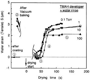 |
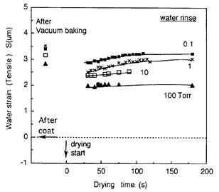 |
|
| Fig.3 Variation of wafer strain versus drying time. The resist films were
treated by developer and subsequently water reise. |
Fig.5 Variation of wafer strain versus drying time.The resisut film was treated by water. |
|
| 1995- 3. | 河合 晃 「原子間力顕微鏡により検出した薄膜の表面力と表面自由エネルギー成分との相関」 日本接着学会誌、31, 237-240 (1995). |
|
| [abstract] 原子間力顕微鏡(AFM)の微細カンチレバーは,薄膜表面へ表面力(主にファンデルワールス力)によって吸着する。この表面力は,接触角法で測定した薄膜の表面自由エネルギーの極性成分に正の相関を示すが,分散成分には感度を持たない。AFMを用いることにより,大気中で非破壊的に薄膜表面の熱力学的挙動を解析する事ができる。 The micro cantilever mounted in atomic force microscopy (AFM) is adsorped to thin film surfaces due to the surface force such as van der Waal's force. This surface force has positive correlation with the polar component of surface free energy measured by the contact angle method. However, it has no sensitivity to the dispersion component. By using AFM, the thermodynamic properties of thin film surface can be analyzed nondestructively in air. |
||
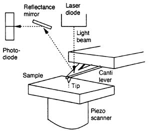 |
 |
|
| Fig.1 The construction of atomic force microscopy system. | Fig.3 Correlation between the surface force detected by AFM and the surface free energy components. |
|
| 1995- 4. | Akira Kawai “Spreading of Water Drop on Geometrical Rough Surface Formed by Photolithography” J. Adhesion Society of Japan, 31, 92-94 (1995). |
|
| [abstract] Dependency of spreading velocity of water drop on roughness is studied. The roughness of surface is controlled by changing the aspect ratio of photoresist micro patterns formed by photolithography. The spreading speed of water drop decreases as the aspect ratio increases. Results obtained in this experiment appear to confirm the Newman’s spreading model. |
||
 |
 |
|
 |
 |
|
| 1995- 5. | Hitoshi Nagata, Atsumi Yamaguchi and Akira Kawai “Characterization of Thin-Film Interference Effect due to Surface Roughness” Jpn. J. Appl. Phys. 34, 3754-3758 (1995). |
|
| [abstract] The normal and diffuse reflectivity from a resist/aluminum system were measured with various resist thicknesses. The average surface roughness σa of aluminum surfaces varied from 5.5 to 10.5 nm upon changing the sputtering conditions. The diffuse reflectivity at the air/aluminum interface increases with surface roughness. This tendency is enhanced as the wavelength of incident light decreases. The interference effect for the resist/aluminum system decreases as the surface roughness increases. This tendency is enhanced when the resist absorptivity decreased. These results are analyzed with using the help of the "Swing" model. KEYWORDS : photolithography, interference effect, photoresist, reflectivity, multiple reflectivity, diffuse reflectance, surface roughness, sputtering, aluminum, LSI |
||
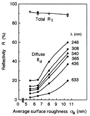 |
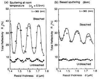 |
|
| Fig.2 The plot of reflectivity of air/aluminium interface versus average surface roughness of aluminium film.The open circlesindicate total reflectivity. The closed circles indicate diffuse reflectivity. The diffuse reflectivity was measured using the integration sphere in the spectrometer. |
Fig.5 Total reflectivity variation of resist/aluminum substrate system with varying resist thickness. The open circles indicate reflectivity from bleached resist. The closed circles indicate reflectivity from unbleached resist. |
|
| 1995- 6. | 河合 晃、熊谷武司、高田雅介 「接触角法により測定した遷移金属薄膜の表面自由エネルギーの分散および極性成分」 日本接着学会誌、31, 307-311 (1995). |
|
| [abstract] 接触角法を用いて、遷移金属薄膜 (Ti, Ni, Cu, Mo, Pd, Ag, W, Pt, Au) の表面自由エネルギーの分散の極性成分を大気中で測定した。分散成分は原子番号の増加とともに周期的に変動し、Cu, Ag, Auで最大値を示した。これは各々3d, 4d, 5dの各軌道が電子で満たされていくことに対応する。極性成分はその大きさによってCu, Pd, Ag, AuとTi, Ni, Mo, W, Ptの二つのグループに分かれた。これはd軌道が電子で完全に満たされた場合と、満たされない場合に各々対応している。これらの結果は、原子間の結合力に及ぼすd軌道電子の影響が表面自由エネルギーの各成分値に強く現れる事を示している。大気中での接触角測定によって、これらの金属自身の性質を検出することが可能である。 Dispersion and polar components of surface free energy of various transition metal films (Ti, Ni, Cu, Mo, Pd, Ag, W, Pt and Au) are determined by the contact angle measurement in air. The dispersion components changes cyclically as the atomic number increases. This result indicates that the 3d, 4d and 5d orbitals are filled out continuously with electrons, respectively. The polar components are separated into two groups. (1)Cu, Pd, Ag and Au, (2)Ti, Ni, Mo, W and Pt, in terms of its magnitude. This result corresponds to the d-orbital structure, closed shell and non‐closed one, respectively. These result indicate that the contribution of d-shell structure to cohesive property of metal has close relationship with the components of surface free energy. By using the contact angle method in air, the property of metal can be detected. |
||
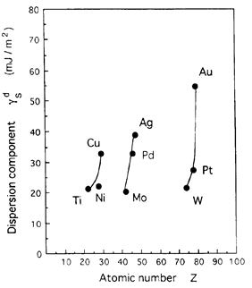 |
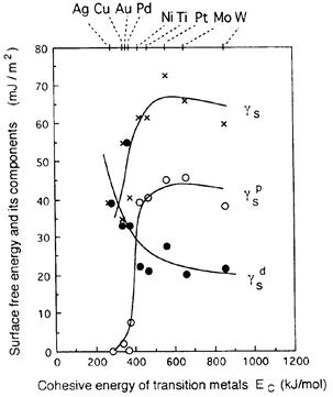 |
|
| Fig.1 A plot of dispersion component of surface free energy versus atomic number of transition metals. | Fig.5 Correlation between surface free energies and cohesive energy of transition metals. |
|
| 1995- 7. | 河合 晃 「表面結露法により検出したAl表面の有機汚染層とフォトレジストパターンの接着性」 日本接着学会誌、31, 354-359 (1995). |
|
| [abstract] 表面結露法(SCM)を用いてAl薄膜表面の有機汚染層を検出し, レジスト微細パターンの接着性を考察した。スパッタリング直後のAl表面には既に有機汚染層が存在し, ウエハの周辺部の汚染が顕著であることがわかった。この有機汚染層は酸素プラズマ処理によりほとんど除去できる。これらはXPS分析, 接触角の測定結果と一致した。有機汚染層の除去により, Al薄膜上のレジストパターンの接着性は改善される。表面結露法は, 固体の表面汚染の解析手法として有効であることを示した。 By the surface condensation method (SCM), the organic contamination of aluminum surface can be detected. Correlation between the surface contamination and adhesion of photoresist micro pattern is studied. The as sputtered aluminum surface has already the organic contamination, mainly, the outer area of wafer. The most of contamination can be easily eliminated by the oxygen plasma treatment. These results can be explained with the XPS and contact angle analysis datas. The adhesion of photoresist micro pattern is improved by eliminating the organic contamination from the aluminum surface. The surface condensation method is available to study the surface contamination of solid surface. |
||
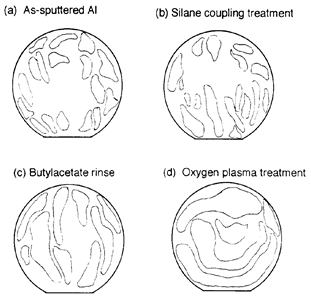 |
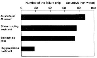 |
|
| Fig.3 The sketches of fringe pattern on the alumintim surfaces. The 6 inches size wafers were used. |
Fig.6 Histgram of the failure patterns of photoresist on the various aluminum stirfaces. | |
| 1995- 8. | Akira Kawai “Adhesion of Resist Micropatterns during Drying after Water Rinse” Jpn. J. Appl. Phys., 34, L1093-L1094 (1995). |
|
| [abstract] The variation of residual strain in photoresist thin films can be detected by a strain gauge with high sensitivity. The adhesion of resist micropattern during drying after water rinse is studied in terms of the residual strain variation. The residual strain of a resist film varies markedly as water is evaporated from the resist surface. In order to improve the resist adhesion, it is important to decrease the residual strain during the drying process. KEYWORDS : Adhesion, residual strain, photoresist, LSI, lithography, pattern development, spin drying, evaporation |
||
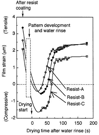 |
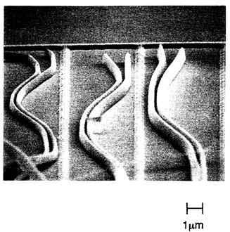 |
|
| Fig.2 Variation of residual strain in the resist films with dryiug time after water rinse. |
Fig.3 SEM micrograph of typical adhesion failure of resist patterns after drying. (resist-A) |
|
| 1995- 9. | Akira Kawai “Adhesion of Micro Window Pattern Formed by Photolithography” J. Adhesion Society of Japan, 31, 360-362, (1995). |
|
| [abstract] Adhesion behavior of photoresist thin film in HF aqueous solution is studied. The photoresist films are fabricated as various micro window shapes by means of photolithography. The envelope shape of silicon-oxide substrate after the HF etching can be controlled by changing the window sizes. |
||
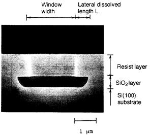 |
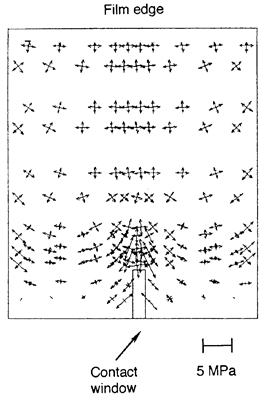 |
|
| Fig.2 The SEM photograph of under-cutting shape of silicon-oxide layer by HF etching. (Cross sectional view) ]Isotropic under-cutting shape can be confirmed. |
Fig.4 The FEM stress analysis around the contact window. (Plane view) All stresses indicate tensile direction. |
|
| 1995-10. | 永田一志、河合 晃 「TMAH水溶液中でレジスト膜に発生した環境応力亀裂」 日本接着学会誌、31, 452-457 (1995). |
|
| [abstract] TMAH (Tetramethylammoniumhydroxide) 水溶液中に浸したフォトレジスト膜に生じる微小亀裂について研究した。この亀裂はウエハ周辺部に多く発生し, その数はレジスト中の残留溶剤量の増加とともに増える。屈折率測定と接触角測定から溶剤蒸発はウエハ中心部より周辺部で顕著であることを確認した。TMAH水溶液とレジストとの反応は溶剤の存在により加速され, これが亀裂分布発生の要因であることを見い出した。 A number of micro cracks occur in photoresist films which are dipped into the TMAH (tetramethylammonium hydroxide) aqueous solution. These micro cracks occur mainly outer area in the wafer and increase by decreasing the resist solvent. By the measurements of refractive index and contact angle, the sufficient solvent evaporation at the outer area of wafer is confirmed. The reaction between resist and TMAH aqueous solution is enhanced by the existence of solvent. The behavior of solvent evaporation is the major factor of crack generation. |
||
 |
 |
|
| Fig.1 The distribution of environmental stress cracking in the film. (6-inches size wafer) |
Fig.2 The cross sectional profile of the cracking measured by surface roughness meter. |
|
| 1995-11. | 永田一志、河合 晃 「レジスト膜上のスピンオンガラス膜に発生する微細亀裂」 日本接着学会誌、31, 498-501 (1995). |
|
| [abstract] リソグラフィー技術の一つである三層レジストプロセス(上層レジスト膜/中間膜/下層レジスト膜構造)において, 中間膜であるシリカガラスに生じる微細クラックの生成メカニズムを考察した。この微細クラックは, シリカガラスのベーク温度が下層レジスト膜のベーク温度を超えた場合に生じる。これは下層レジスト膜からの溶媒の蒸発によりシリカガラス膜に応力がかかることが原因であると考えられる。下層レジスト膜の熱に対する軟化性を増すことで, 微細クラックの発生を防止できる。 The tri-layer resist process is one of the useful lithography techniques for submicron fabrication. In the tri-layer structure (top-resist layer/middle layer/ bottom-resist layer), the generation mechanism of micro-crack in the spin-on-glass (SOG) layer has been studied. The micro-crack occurs when the baking temperature of SOG layer is higher than that of bottom-resist layer. This is because the stress generation in the SOG layer occurs by the evaporation of resist solvent from bottom-resist layer. The thermal softening of the bottom-resist layer has an effect to prevent the micro-crack generation. |
||
 |
 |
|
 |
||
1994年 9報
| 1994- 1. | 河合 晃、永田一志 「有機スピンオンガラス上でのフォトレジストの濡れ不良」 日本接着学会誌、30, 582-585 (1994). |
|
| [abstract] 大規模集積回路 (LSI) の製造技術の一つである多層レジストリソグラフィーにおいて,上層レジストのスピン塗布時に発生する大面積の濡れ不良が問題となっている。これは有機SOG膜上の微小欠陥によってレジスト膜の連続性が崩れることが原因で発生する。有機SOG膜はメチル基(-CH3)を含んでおり,その濃度は焼成温度の増加とともに減少するが,SOG焼成温度が175℃以下になるとレジストの濡れ不良は消成するが,この現象を各膜の表面自由エネルギーを用いて考察する。 The wetting failure of photoresist is a major problem for the multilayer-resist in large scale integrated circuit (LSI) fabrication. The wetting failure occurs when a micro particle exists on the spin-on-glass (SOG) surface. The concentration of (CH3-) group decreases as the baking temperature increases. No wetting failure occurs under the baking temperature of 175℃. This phenomenon is discussed by using surface free energy of each surface. |
||
 |
 |
|
| Fig.2 The photograph of wetting failure of photoresist. The solid core can be observed at the center of the failure area. |
Fig.3 Correlation between number of wetting failure and baking temperature of the organic SOG film. |
|
| 1994- 2. | Akira Kawai, Hitoshi Nagata and Masasuke Takata, “Measurement Method of Adhesion Strength between Inorganic Materials and Polymer by Using Atomic Force Microscopy” J. Ceramic Society of Japan, 102, 1102~1104 (1994). |
|
| [abstract] A new application of the interaction phenomenon between tip and surface to practical adhesive behavior is studied. The interactive energy between two films can be estimated from the measured data of attractive force by atomic force microscopy (AFM). The adhesive strength between inorganic materials and polymer is closely related to the estimated value of interactive energy. The adhesive strength can be estimated by using a nondestructive method. Key-words : Atomic force microscopy, Surface force, Adhesion, Elastic energy, Destruction, Photoresist, Cantilever tip |
||
 |
||
 |
||
| 1994- 3. | 河合 晃、永田一志、高田雅介 「レジスト微細パターン内の熱応力分布と接着特性」 日本接着学会誌、30, 549-554 (1994). |
|
| [abstract] レジストパターン内に発生する熱応力と接着特性との相関を調べた。レジストパターンの平面形状に対応して熟応力が分布する。特に,凹凸の形状を有するパターンにはそれぞれ圧縮応力,引っ張り応力の集中が生じる。酸化膜基板のサイドエッチングは,この応力集中により大きく影響を受ける事を見い出した。 The correlation between the thermal stress and the adhesion behavior of photoresist was studied. The thermal stress distributed along with the planer shape of the resist pattern. Compressive and stresses were especially concentrated at the inner and the outer corners, respectively. It is found that the side-etching of the thermal oxide substrate has a close relationship to these stress concentration. |
||
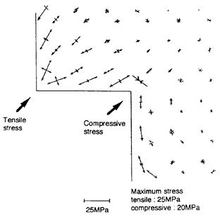 |
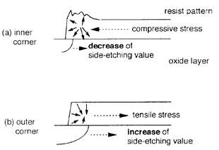 |
|
| Fig.4 The principal stress distribution in a photoresist pattern which has two different corners. The distribution was calculated by a two-dimensional finite element method. |
Fig.7 Scematical diagram for explaining the relationship between thermal stress and variation of side etching value. (a)inner corner. (b)outer corner. |
|
| 1994- 4. | Akira Kawai, Hitoshi Nagata, “Wetting Behavior of Liquid on Geometrical Rough Surface Formed by Photolithograpy” Jpn. J. Appl. Phys. 33, L1283-L1285 (1994). |
|
| [abstract] The effect of roughness on the wettability is studied. The rough surface is constructed with photoresist micropatterns which are formed by photolithography. The aspect ratio is defined as the length ratio between the pattern space and its height. Contact angles of three kinds of liquids, pure water, diiodomethane and ethylene glycol, increase and saturate with the increase of the aspect ratio. The wetting behavior of pure water of which higher surface energy is extremely complex. KEYWORDS : wetting, adhesion, photoresist, LSI, lithography, surface free energy, contact angle, thermodynamics |
||
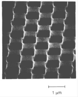 |
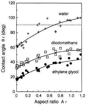 |
|
| Fig.2 SEM micrograph of the photores ist micropatterns formed by photolithography. |
||
| 1994- 5. | Akira Kawai, Hitoshi Nagata, “Wetting Failure of Photoresist on Spin-On-Glass (SOG) Substrate by Spin Coating” Jpn. J. Appl. Phys. 33, L1355-L1357 (1994). |
|
| [abstract] The wetting failure of photoresist occurs during the spin-coating process on the spin-on-glass (SOG) surface. The SOG surface has relatively low surface free energy. By treating the SOG surface with an alkaline aqueous solution prior to the photoresist coating, wetting failure can be prevented. The alkali treatment has the effect of increasing the surface free energy of SOG film, especially in its polar component. The spreading work WS changed from a positive to negative value by the alkali treatment, which can explain the prevention of the wetting failure. KEYWORDS : wetting, surface free energy, contact angle, photoresist, spin-on-glass, spin coating, thermodynamics, condensation, photolithography, trilayer resist lithography, LSI |
||
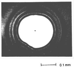 |
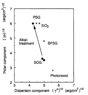 |
|
| Fig.1 A photograph of wetting failure by optical observation. A solid core can be observed in the center of each wetting failure. |
Fig.2 The component map of surface free energy for the various films. |
|
| 1994- 6. | Akira Kawai, Hitoshi Nagata and Masasuke Takata, “Shrinkage Effect of Local Area of Polymer Film on Adhesion Behavior” Jpn. J. Appl. Phys. 33, L973-L974 (1994). |
|
| [abstract] We report a dependency of adhesion behavior in HF aqueous solution on film shrinkage of local area in a photoresist/silicon-oxide system. Micro window patterns of photoresist film are formed by means of photolithography. Side etching length of silicon-oxide substrate increases and saturates with the shrunken area of photoresist film. Adhesion strength can be expressed as a function of shrunken area. KEYWORDS : adhesion, thermal stress, photoresist, shrinkage, tensile stress, lithography, intrusion, elasticity |
||
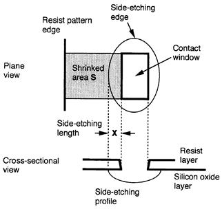 |
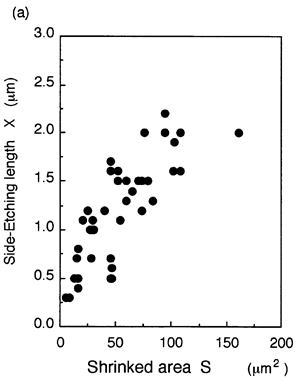 |
|
| Fig.1 Schematic diagram of side-etching behavior of silicon-oxide subsrate. (Cross-sectional view): undercut shape of substrate. (Plane): shrinkage of local resist area between pattern edge and contact window. |
Fig.2 Adhesion of resist/SiO2 system. (a): A plot of side-etching length
X versus shrinked area of resist S. |
|
| 1994- 7. | Akira Kawai, Hitoshi Nagata, Hiroaki Morimoto and Masasuke Takata, “Adhesion of Photoresist Pattern Baked at 80 to 325℃ to Inorganic Solid Surface” Jpn. J. Appl. Phys. 33, L146-L148 (1994). |
|
| [abstract] Adhesion of positive photoresist films which were baked at 80 to 325℃ on inorganic surfaces is analyzed with respect to thermodynamics. The peeling strength of resist/solid surface systems shows a minimum value for a baking temperature range from 150 to 200 ℃. It is found that the hydrogen bonding interaction of resist/surface system mainly affected the adhesion phenomena. KEYWORDS : adhesion, photoresist, LSI, lithography, surface free energy, peeling, contact angle, thermodynamics, van der Waals force |
||
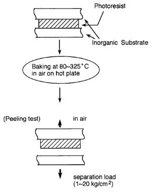 |
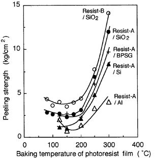 |
|
| Fig.1 Schematic flow chart for measuring system of peeling strength. | Fig.2 Dependency of peeling strength on baking temperature of photoresist. |
|
| 1994- 8. | Hitoshi Nagata, Akira Kawai, Hiroaki Morimoto and Masasuke Takata, “Blister Formation at photoresist-Substrate Interface” Jpn. J. Appl. Phys. 33, 3635-3639 (1994). |
|
| [abstract] We report the formation mechanism of a blister at the photoresist-substrate interface during exposure to ultraviolet (UV) light. It is found that the blister formation strongly depends on the following factors: (i) photoactive-compound (PAC) concentration of the photoresist film and (ii) adhesion energy between the photoresist film and the substrate. Formation parameter U, which represents the difference between the adhesion energy and the strain energy of the photoresist film, can be utilized for predicting the blister formation. KEYWORDS : adhesion, surface free energy, blister, photoresist, LSI, inorganic substrate, stress |
||
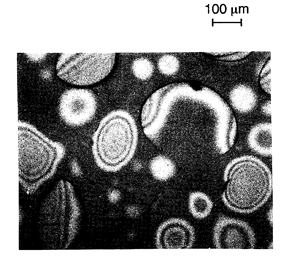 |
 |
|
| Fig.7 Correlation between number of blisters and formation parameter U (Si substrate). |
||
| 1994- 9. | Akira Kawai, Hitoshi Nagata, Hiroaki Morimoto and Masasuke Takata, “Local Peeling of Photoresist Film during Ultraviolet Light Exposure” Jpn. J. Appl. Phys. 33, L149-L151 (1994). |
|
| [abstract] Circular peels are formed during exposure of the photoresist film to ultraviolet (UV) light. Dependency of peel formation in photoresist film on adhesion energy is investigated. The value of adhesion energy is derived from the measurement value of surface free energy. The surface free energy of inorganic substrates used for the investigation is between the values of 46.5 and 62.6 dyn/cm. It is found that the number of peels decreases as the adhesion energy increases. Peel formation can be explained by using the adhesion energy. KEYWORDS : adhesion, surface free energy, peel, photoresist, LSI, defect, strain, inorganic,substrate |
||
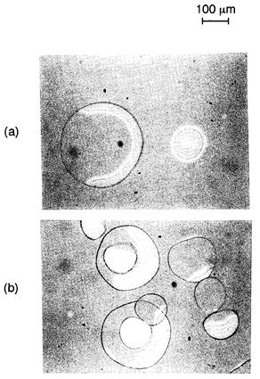 |
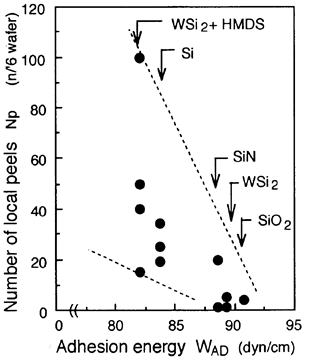 |
|
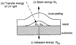 |
||
 |
||
1983年-1993年 8報
| 1993- 1. | Akira Kawai, Hitoshi Nagata and Masasuke Takata “Dependency of Adhesion Behavior on Thermal Stress Distribution in Photoresist Micropatterns” Jpn. J. Appl. Phys. 32, 1020-1024 (1993). |
|
| [abstract] We report an excellent correlation between adhesive behavior in HF aqueous solution and internal distribution of thermal stress in a photoresist pattern. The stress distribution was analyzed using the two-dimensional finite element modeling in the cross section of the photoresist pattern. The large envelope shape, which indicates weak adhesion, was confirmed by the concentration of stress at the resist-substrate interface. In particular, the hardened layer of the photoresist pattern surface has the effect of forming the two-step shape of the etching envelope due to isotropic and lateral intrusion. KEYWORDS : adhesion, thermal stress, rheology, finite element modeling, photoresist, tensile stress, stress concentration.lithography, intrusion, elasticity |
||
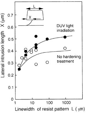 |
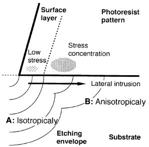 |
|
| Fig.2 Dependency of lateral intrusion length on linewidth of resist pattern. |
Fig.5 A schematic model explaining the formation of the two-step envelope shape during HF etching. |
|
| 1992- 1. | Akira Kawai, Hitoshi Nagata and Masasuke Takata “Adhesion of Photoresist Micropattern to Aluminum Substrate in Alkaline Aqueous Solution” Jpn. J. Appl. Phys. 31, 1933-1939 (1992). |
|
| [abstract] The purpose of this study is to analyze the fracture mechanism of adhesive bonding between a photoresist micropattern and an aluminum surface in an alkaline aqueous solution. Various surface treatments are performed on the aluminum surface prior to photoresist coating in order to control surface free energy and the thickness of the surface layer, which respectively relate to the two well-known fracture models: (i) debonding at the resist-aluminum interface and (ii) cohesive failure in the surface layer. Surface free energy is determined by means of the contact angle method. The thicknesses of the grease and oxide layers on the aluminum surface are obtained by means of ellipsometry. The results do not provide further evidence of a correlation between practical adhesive strength and surface free energy. It is also found that adhesive strength decreases with increases in surface oxide thickness. The interpretation of this is that bond failure does not take place at the interface between the aluminum and photoresist, but occurs in the oxide layer, which acts as a weak boundary layer, on the aluminum surface. KEYWORDS : adhesion, weak boundary layer, LSI, photolithography, surface free energy, contact angle, aluminum |
||
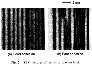 |
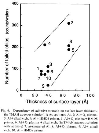 |
|
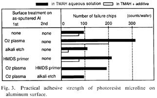 |
||
| 1992- 2. | Akira Kawai, Hitoshi Nagata and Masasuke Takata “Adhesion of Photoresist Pattern Baked at 80 to 325℃ in Tetramethyl-ammonium- hydroxide Aqueous Solution” Jpn. J. Appl. Phys. 31, 3725-3730 (1992). |
|
| [abstract] Adhesion characteristics of a photoresist thin film baked onto spin-on SiO2 layer at 80 to 325℃ are studied in a Tetramethyl-ammonium- hydroxide(TMAH) developer. The maximum value of adhesion strength is observed in the temperature range of 150 to 250℃. It is found that the surface energy model cannot explain all of the experimental results. The following two models are introduced as new adhesion factor: (i) decrease of surface energy of the TMAH developer due to dissolution of photoresist into it above 250℃ and (ii) decrease of mechanical strength of a photoresist pattern by swelling under 150℃. KEYWORDS : adhesion, photoresist, lithography, surface energy, swelling, intrusion, pattern development, contact angle, thermodynamics |
||
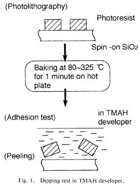 |
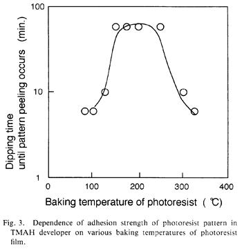 |
|
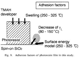 |
||
| 1992- 3. | Akira Kawai, Hitoshi Nagata and Masasuke Takata “Characterization of Surface Energetic Behavior by Atomic Force Microscopy” Jpn. J. Appl. Phys. 31, L977-L979 (1992). |
|
| [abstract] Inorganic solid surface which have various surface free energies, 30~65 dyn/cm, were probed using a Si3N4 cantilever tip. It was found that the attractive force(~10-7N), which is generated when a cantilever tip moves away from a solid surface after making contact, is more sensitive to the behavior of surface free energy than that (~10-9N) which is generated when the tip moves toward the surface. The relationship between the elastic potential energy of the cantilever and the adhesion energy of the tip-surface system is also discussed. KEYWORDS : atomic force microscopy, van der Waal’s force, surface force, thermodynamics, surface free energy, contact angle, adhesion, elastic potential energy |
||
 |
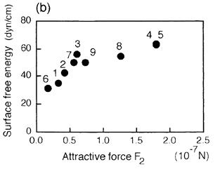 |
|
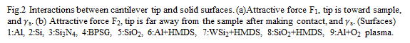 |
||
| 1992- 4. | Akira Kawai, Jinzou Watanabe, Hitoshi Nagata and Masasuke Takata, “Dependence of Offset Error on Overlay Mark Structures in Overlay Measurement” Jpn. J. Appl. Phys. 31, 385-390 (1992). |
|
| [abstract] Measurement precision, especially the offset error in the automatic measurement technique of overlay, was studied for sub-half-micron device manufacturing. Experimental data showed that the offset error depended on the cross-sectional structure rather than the reflectivity or the toughness of the measurement marks. Dependence of the offset error upon equipment factors, e.g., the incident angle of illumination, was also studied. The depth of focus was considerably increased up to 1.5 mu m on the LSI wafers with well-aligned light. This paper also shows an offset error on critical levels in sub-half-micron device manufacturing. KEYWORDS : overlay, misregistration, LSI, depth of focus, illumination angle, reflectivity, surface roughness |
||
 |
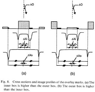 |
|
| 1991- 1. | Akira Kawai, Hitoshi Nagata, Haruhiko Abe and Masasuke Takata, “Adhesion between Photoresist and Inorganic Substrate” Jpn. J. Appl. Phys. 30, 121-125 (1991). |
|
| [abstract] Adhesion strength of a photoresist during pattern development decreases as penetration of an alkaline aqueous solution into the photoresist film increases. The penetration is accelerated by increasing the quantity of residual solvent in the photoresist film. Resistance measurements confirmed the penetration. The tensile stress of photoresist films increases as the penetration increases. The creation of inner stress also causes adhesion failure during HF etching. These phenomena cannot be explained by a balance model of surface energy. Therefore, we conclude that the increase in tensile stress causes adhesion loss during both pattern development and HF etching. KEYWORDS : adhesion, surface energy, photoresist, density, penetration, solvent, stress, semiconductor |
||
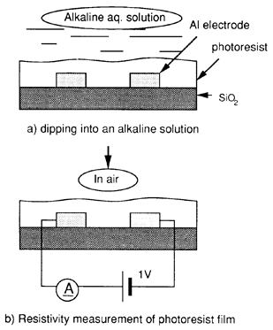 |
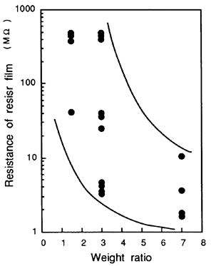 |
|
| Fig.1 Schematic diagram of the system for measuring resistanceof the photoresist film. |
Fig.7 Resistance of the photoresist films after dipping in alkaline aqueous solution. |
|
 |
||
| Fig.9 The model of adhesion failure caused by diffusion of alkaline aqueous solution. | ||
| 1989- 1. | Hitoshi Nagata and Akira Kawai, “Characteristics of Adhesion between Photoresist and Inorganic Substrate” Jpn. J. Appl. Phys. 28, 2137-2141 (1989). |
|
| [abstract] The adhesion of positive photoresist film to some inorganic substrates used as LSI substrate material in dry and wet conditions has been investigated based on surface chemistry. The method of surface energy treatment is used to predict the adhesion energy. The contact angle method is used to measure the surface energy of each substrate. The correlation between the value of two components of surface energy, the polar and the dispersion parts, and adhesion strength is discussed. It is important to control the polar part of surface energy of a substrate in order to achieve high adhesion strength. KEYWORDS : adhesion, surface tension, contact angle, photoresist, intrusion, dynamic memory, semiconductor |
||
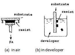 |
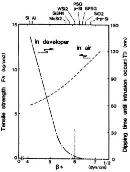 |
|
| Fig.3 Test systems for adhesion strength in cross section. | ||
| 1983- 1. | Shoichi Okamoto, Akira Kawai, Kenkichiro Kobayashi, Masasuke Takata, TsutomuYamashita and Shiro Yamashita, “Synthesis of TiB2 by High-Dose Implantation of Boron Ions Titanium Films” J. American Ceramic Soc., 66, c-78 (1983). |
|
| [abstract] Boron ions were implanted at room temperature in Ti films at a high dose (7.1×10¹⁷ and 2.3×10¹⁸ ions/cm2). The formation of TiB2 films was confirmed by X-ray diffraction. Boron concentration profiles in implanted films were studied by secondary-ion mass spectrometry. |
||
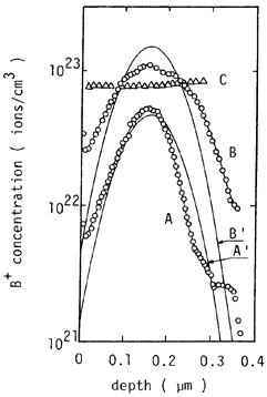 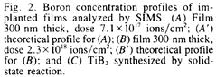 |
||